Supercharge Your Innovation With Domain-Expert AI Agents!

A kind of ldmos transistor structure and preparation method thereof

A technology of transistors and semiconductors, applied in semiconductor/solid-state device manufacturing, electric solid-state devices, semiconductor devices, etc., can solve problems such as unstable working environment of LDMOS devices, large area occupied by LDMOS devices, uneven distribution of electric field in the gate region, etc. , to achieve the effects of reduced size, increased charge and discharge rate, and compact distribution

Active Publication Date: 2017-07-14
SEMICON MFG INT (SHANGHAI) CORP
View PDF3 Cites 0 Cited by
  • Summary
  • Abstract
  • Description
  • Claims
  • Application Information

AI Technical Summary

Problems solved by technology

[0005] In view of the above-mentioned shortcomings of the prior art, the object of the present invention is to provide an LDMOS transistor structure and its preparation method, which are used to solve the problem of large lead-out resistance of the gate region and uneven electric field distribution on the gate region in the prior art. The working environment of the LDMOS device is unstable, which leads to the problem of the breakdown of the LDMOS device and the excessive area occupied by the LDMOS device in the entire chip, which limits the vertical width of the gate on the active region, making the charge and discharge of the device work slowdown problem

Method used


Image

  • A kind of ldmos transistor structure and preparation method thereof
  • A kind of ldmos transistor structure and preparation method thereof
  • A kind of ldmos transistor structure and preparation method thereof

Examples


Embodiment 1

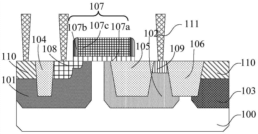
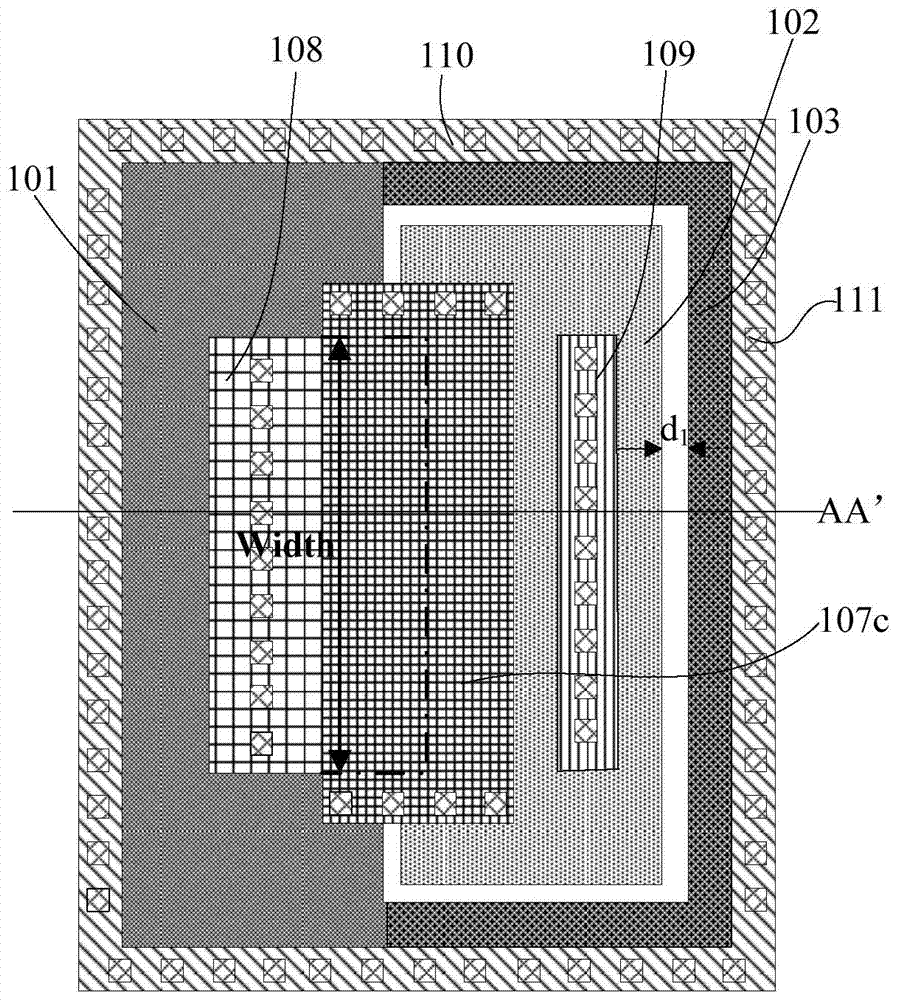
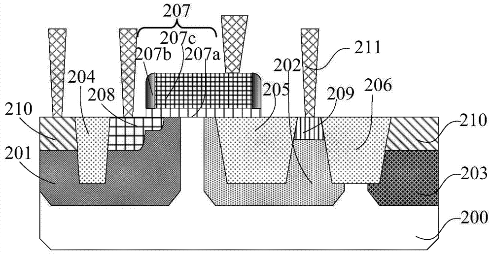
[0048] see figure 2 , is a schematic structural view of the LDMOS transistor of the present invention, the LDMOS transistor structure at least includes: a semiconductor substrate 200; a first high voltage well region 201, a second high voltage well region 202 and a first high voltage well region 202 formed in the semiconductor substrate 200 The third high-voltage well region 203; the doping type of the second high-voltage well region 202 is opposite to that of the first high-voltage well region 201 and the third high-voltage well region 203; formed in the first high-voltage well region The first shallow trench isolation region 204 in 201; the second shallow trench isolation region 205 formed in the second high voltage well region 202 and the second high voltage well region 202 and the third high voltage well The third shallow trench isolation region 206 between regions 203; the gate region 207 formed on the semiconductor substrate 200 and covering part of the first high volta...

Embodiment 2

[0092] In this embodiment, the preparation method of the PLDMOS transistor is taken as an example. The preparation steps of the PLDMOS transistor are exactly the same as the preparation steps of the NLDMOS transistor in Example 2. The difference between the two mainly lies in:

[0093] In step 1), the provided substrate is an N-type substrate. During the process of forming the first high-voltage well region 201 , the second high-voltage well region 202 and the third high-voltage well region 203 , the first high-voltage well region 201 and the third high-voltage well region 203 are formed. N-type ion implantation is performed on the third high-voltage well region 203, and P-type ion implantation is performed on the second high-voltage well region 202;

[0094] In step 4), during the process of forming the source region 208 and the drain region 209, P-type ion implantation is performed on them, and during the process of forming the body lead-out region 210, N-type ion implantatio...


PUM


Abstract

The present invention provides an LDMOS transistor structure and a preparation method thereof, at least comprising a semiconductor substrate, a first high voltage well region, a second high voltage well region, a third high voltage well region, a first shallow trench isolation region, and a second shallow trench an isolation region, a third shallow trench isolation region, a source region, a drain region, a body lead region, a gate region and a contact hole, and the contact holes are respectively arranged in the source region, the drain region, the body lead region and the gate region Above, the contact holes arranged on the gate region are vertically distributed on one side of the gate polysilicon layer above the second shallow trench isolation region. In the present invention, the contact holes are rearranged and distributed on the gate polysilicon layer above the second shallow trench isolation region, so that the electric field distribution on the gate region is more uniform, and the intersection of the active region and the gate region will not be reached. Any negative impact, from the design to reduce the area occupied by the LDMOS device in the entire chip, in order to achieve the final customer chip size reduction.

Description

technical field [0001] The invention relates to the technical field of semiconductor devices, in particular to an LDMOS transistor structure and a preparation method thereof. Background technique [0002] LDMOS (Laterally Diffused MOSFET, laterally diffused MOS transistor) is a power MOS transistor. Due to its ability to withstand high voltage (such as 24V) and high current density (such as 2A / mm) in the BCD (Bipolar-CMOS-DMOS) process 2 ), so LDMOS devices are usually used as switching tubes as the final output driver. The withstand voltage capability of the LDMOS device is proportional to the size of the lightly doped region and the distance of the level drop. The higher the design withstand voltage, the larger the required size. Therefore, the LDMOS device that can withstand high voltage and high current must occupy a large area. block chip area. [0003] Figure 1a It is a schematic structural diagram of an LDMOS transistor in the prior art, Figure 1b for Figure 1a...

Claims


Application Information

Patent Timeline
Patent Type & Authority Patents(China)
IPC IPC(8): H01L23/48H01L21/336H01L21/60
Inventor 曹国豪
Owner SEMICON MFG INT (SHANGHAI) CORP
Features
  • R&D
  • Intellectual Property
  • Life Sciences
  • Materials
  • Tech Scout
  • Unparalleled Data Quality
  • Higher Quality Content
  • 60% Fewer Hallucinations
Learn More