LED (light emitting diode) with dual-reflector structure and manufacturing method of LED with dual-reflector structure

A technology of light-emitting diodes and double mirrors, which is applied to electrical components, circuits, semiconductor devices, etc., can solve the problems of low light extraction efficiency and poor N-surface current expansion effect, and achieve simple manufacturing process, good product stability, and high The effect of reflectivity

Active Publication Date: 2015-06-03
YANGZHOU CHANGELIGHT
View PDF4 Cites 2 Cited by
  • Summary
  • Abstract
  • Description
  • Claims
  • Application Information

AI Technical Summary

Problems solved by technology

The traditional reflective layer structure is a single layer, and a mirror with high reflectivity is made on the P side of the epitaxial structure. However, due to the poor current spreading effect on the N side, a larger electrode needs to be set on the N side to assist the current expansion. , it will inevitably cause light shading, and the electrode will absorb part of the light at the same time, resulting in low light extraction efficiency

Method used


Image

  • LED (light emitting diode) with dual-reflector structure and manufacturing method of LED with dual-reflector structure
  • LED (light emitting diode) with dual-reflector structure and manufacturing method of LED with dual-reflector structure
  • LED (light emitting diode) with dual-reflector structure and manufacturing method of LED with dual-reflector structure

Examples


Embodiment Construction

[0040] One, the manufacturing steps of the present invention are as follows:

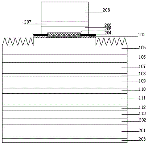
[0041] 1. If figure 1 As shown, a transition layer 102, an N-GaInP cut-off layer 103, an N-GaAs ohmic contact layer 104, an N-AlGaInP roughening layer 105, and an N-AlGaInP current spreading layer 106 are sequentially grown on a temporary GaAs substrate 101 by using MOCVD equipment. , N-AlGaInP confinement layer 107, MQW multiple quantum well active layer 108, P-AlGaInP confinement layer 109, buffer layer 110, P-GaP current spreading layer 111.

[0042] Wherein the N-GaAs ohmic contact layer 104 preferably has a thickness of 60nm, the doped impurity element is Si, and the doping concentration is 8×10 18 cm -3 above to ensure a good electrical contact on the N side.

[0043] The preferred thickness of the P-GaP current spreading layer 111 is 3000nm, the doped impurity element is Mg, and the doping concentration is 7×10 18 cm -3 above to ensure a good electrical contact on the P side.

[0044]...


PUM


Abstract

The invention discloses an LED (light emitting diode) with a dual-reflector structure and a manufacturing method of the LED with dual-reflector structure and belongs to the technical field of photoelectronic technique. A bonding layer epitaxial wafer is bonded with a permanent substrate; a temporary substrate, a transition layer and a cut-off layer are removed; a graphical N-GaAs ohmic contact layer and an extended electrode are made; the LED is characterized in that a SiO2 conductive porous layer with a plurality of through holes is formed in one side of a P-GaP current extension layer of the epitaxial layer, and then a mirror surface is formed through vapor deposition; a SiO2 dielectric film, a mirror layer and a main electrode formed by a barrier layer and a wire solder layer are sequentially made on an N-AlGaInP armoring layer. According to the LED with the dual-reflector structure, the light emitted by the LED escapes by undergoing multiple reflections and refractions, and a schottky junction is formed due to the dielectric film made under the main electrode, so that the ineffective injection of current is reduced, and the light output efficiency of the LED is effectively improved.

Description

technical field [0001] The invention belongs to the technical field of optoelectronics, in particular to the technical field of manufacturing AlGaInP quaternary light-emitting diodes. Background technique [0002] Quaternary AlGaInP is a semiconductor material with direct wide bandgap, which has been widely used in the preparation of various optoelectronic devices. Since the light-emitting band of the material can cover the red to yellow-green bands of visible light, the high-brightness light-emitting diodes made of visible light have attracted extensive attention. Quaternary AlGaInP red high-brightness light-emitting diodes have been widely used in many aspects such as outdoor displays, traffic lights, and car lights. Compared with AlGaInP LED chips with ordinary structures, high-brightness AlGaInP chips use bonding technology to realize substrate replacement, and use silicon substrates with good thermal performance (the thermal conductivity of silicon is about 1.5W / K....

Claims


Application Information

Patent Timeline
Patent Type & Authority Applications(China)
IPC IPC(8): H01L33/10H01L33/06H01L33/14
Inventor 马祥柱白继锋杨凯李俊承张双翔张银桥王向武
Owner YANGZHOU CHANGELIGHT
Why Eureka
Try Eureka