An optical interconnect substrate for use in spacecraft and military computers and its manufacturing method

A computer and spacecraft technology, applied in the field of optical interconnect substrate and its manufacturing, to reduce light wave absorption and scattering loss, meet the needs of high-speed data transmission, and easy to achieve

Active Publication Date: 2016-05-11
NO 771 INST OF NO 9 RES INST CHINA AEROSPACE SCI & TECH
View PDF6 Cites 0 Cited by
  • Summary
  • Abstract
  • Description
  • Claims
  • Application Information

AI Technical Summary

Problems solved by technology

[0004] The optical interconnection substrates at home and abroad are basically PCB boards, and there is no optical interconnection technology based on LTCC substrates.

Method used


Image

  • An optical interconnect substrate for use in spacecraft and military computers and its manufacturing method
  • An optical interconnect substrate for use in spacecraft and military computers and its manufacturing method
  • An optical interconnect substrate for use in spacecraft and military computers and its manufacturing method

Examples


Embodiment Construction

[0039] In order to make the purpose, technical solution and advantages of the present invention clearer, the technical solution of the present invention will be described in detail below in conjunction with the accompanying drawings.

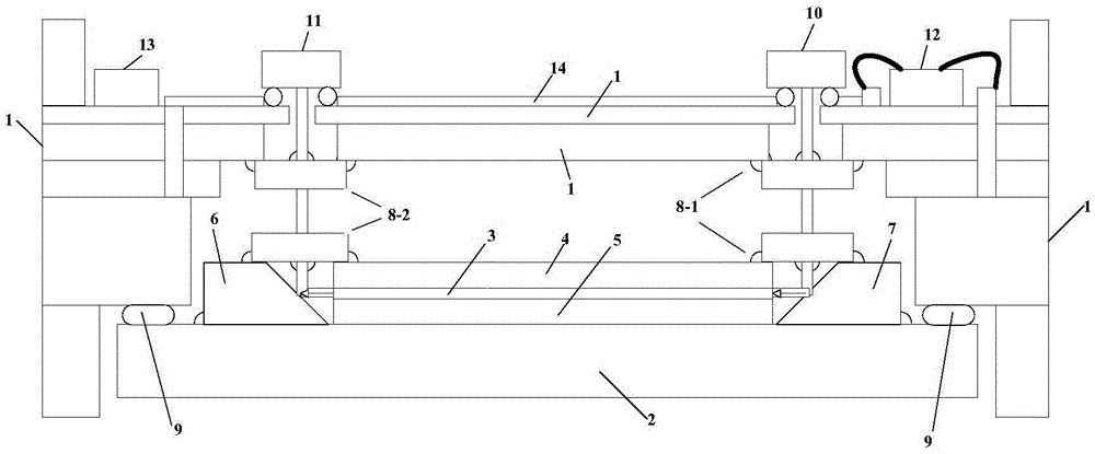
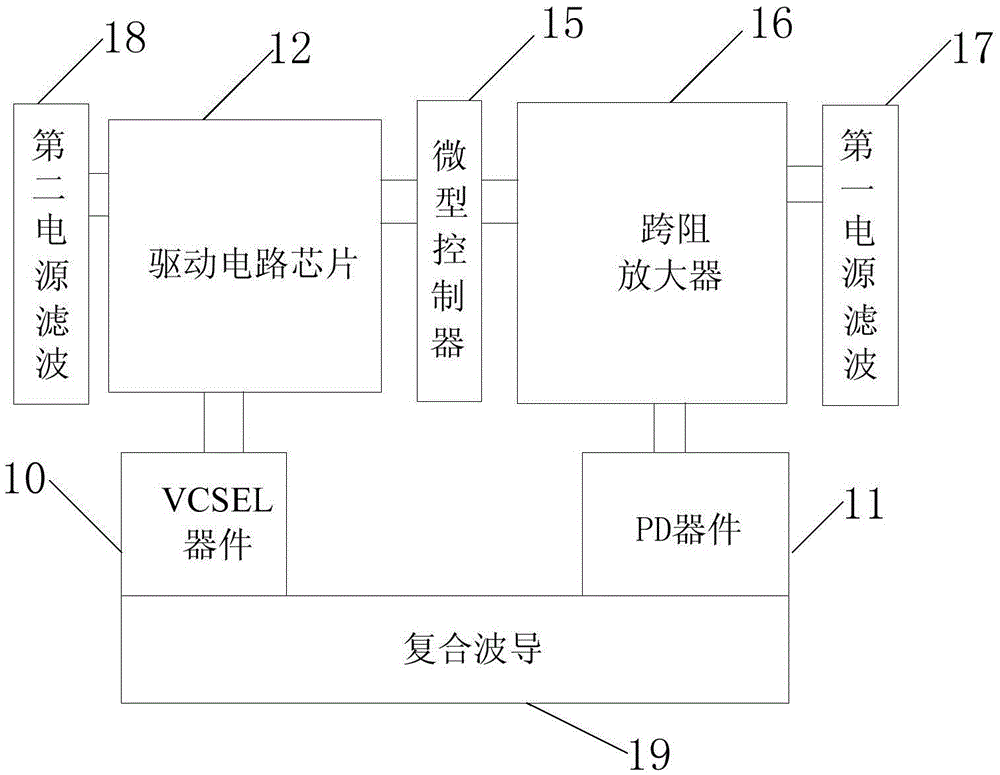
[0040] see figure 1 , an optical interconnection substrate for spacecraft and military computers, comprising a first reflector 7, a second reflector 6, a first microlens array 8-1, a second microlens array 8-2, and a launch assembly , a receiving component, a silicon wafer 2 polished on one side, and an LTCC substrate 1 with a cavity on one side, wherein the transmitting component integrates a VCSEL device 10, a VCSEL interface circuit board and a driving circuit chip 12; the receiving component integrates a PD device 11 , PD interface circuit board, drive circuit chip; The cavity of described LTCC substrate 1 is provided with the silicon wafer 2 of single-sided polishing, and the surface roughness of the polished surface of silicon wafer 2 is l...


PUM


Abstract

The invention discloses an optical interconnection substrate applied to a spacecraft and a military computer and a manufacturing method thereof. The optical interconnection substrate comprises a transmitting component, a receiving component and an LTCC (Low Temperature Co Fired Ceramic) substrate provided with a cavity, the cavity of the LTCC substrate is internally provided with a single side polished silicon wafer, and a polishing surface of the silicon wafer is provided with a composite waveguide; one end of the composite waveguide is provided with a first reflector, and the other end of the composite waveguide is provided with a second reflector; another side of the LTCC substrate is assembled with a VCSEL (Vertical Cavity Surface Emitting Laser) device in the transmitting component and a PD (Potential Difference) device in the receiving component, a first micro-lens array is arranged between the VCSEL device and the first reflector, and a second micro-lens array is arranged between the PD device and the second reflector. The LTCC optical interconnection substrate provided by the invention has the characteristics of being smaller in volume, lighter in weight and higher in integration density, thereby being applicable to manufacturing the spacecraft and the military computer, and being easier to realize an assembling process of a photoelectric component.

Description

technical field [0001] The invention belongs to the technical field of semiconductor hybrid integrated circuits, and in particular relates to an optical interconnect substrate used in spacecraft and military computers and a manufacturing method thereof. Background technique [0002] With the process of digitization, the processing, storage and transmission of data have been developed rapidly. With the improvement of the performance of warships and starships, the requirements for data transmission capabilities are also getting higher and higher, and there is an urgent need for real-time and high-speed collection of complex information from various aspects, data processing and automatic control. Such as the observation, recording, display and storage of high-speed motion or transient processes; the recognition and precise measurement of the shape and size of complex two-dimensional and three-dimensional objects; the analysis and interpretation of macroscopic or ultra-fine grap...

Claims


Application Information

Patent Timeline
Patent Type & Authority Patents(China)
IPC IPC(8): G02B6/43
Inventor 姜伟郑东飞李建国
Owner NO 771 INST OF NO 9 RES INST CHINA AEROSPACE SCI & TECH
Why Eureka
Try Eureka