Wafer repetitive lithography defect inspection and analysis method, system and wafer production method

A defect inspection and analysis method technology, which is applied in semiconductor/solid-state device testing/measurement, electrical components, circuits, etc., can solve problems such as easy missed or false detection, and difficult to effectively detect repetitive lithography defects on wafers. Achieve the effect of avoiding missed or false detection, reducing the risk of shipment, and high convenience

Active Publication Date: 2017-08-04
BYD SEMICON CO LTD +1
View PDF3 Cites 0 Cited by
  • Summary
  • Abstract
  • Description
  • Claims
  • Application Information

AI Technical Summary

Problems solved by technology

[0006] In order to solve the problem that it is difficult to effectively detect the repetitive lithography defects of the wafer caused by the traditional manual microscope inspection, and it is easy to miss or misdetect the problem, the embodiment of the present invention provides a method for inspection and analysis of the repetitive lithography defects of the wafer, Wafer repetitive lithography defect inspection and analysis system and wafer production method

Method used


Image

  • Wafer repetitive lithography defect inspection and analysis method, system and wafer production method
  • Wafer repetitive lithography defect inspection and analysis method, system and wafer production method
  • Wafer repetitive lithography defect inspection and analysis method, system and wafer production method

Examples


Embodiment 1

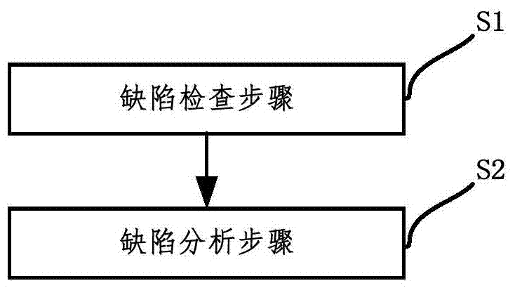
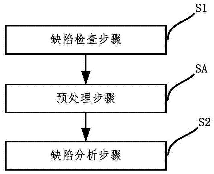
[0059] like figure 1 As shown, this example provides a wafer repetitive lithography defect inspection and analysis method, including the following steps:

[0060] S1. Defect inspection step: after the lithography process of a certain batch of wafers is completed, N wafers are selected from the batch of wafers, and the defects on the selected wafers are scanned in full to obtain the Defect information of the selected wafer; the defect information includes position information and size information of the defect;

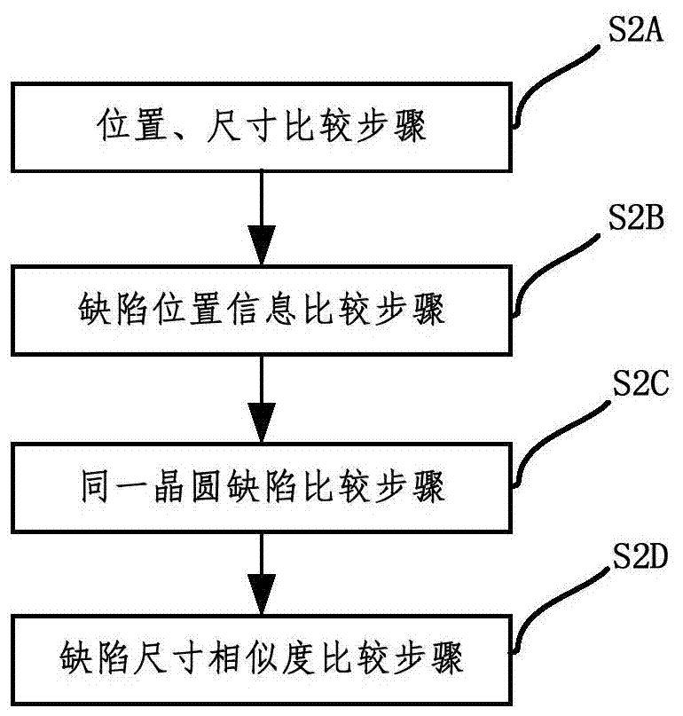
[0061] S2, defect analysis step: compare the position information and size information of the selected wafer defects;

[0062] If there are defects with consistent position information and size information on the selected wafers, it is determined that the batch of wafers has repetitive lithography defects in the lithography process;

[0063] If there is no defect with consistent position information on the selected wafers, it is determined that the batch of wafers ha...

Embodiment 2

[0100] This example provides a wafer production method, which includes the following steps: after a certain batch of wafers is finished with a lithography process, repetitive lithography defect inspection and analysis are performed on the wafers;

[0101] If there are no repetitive lithography defects, continue to follow-up production;

[0102] If there is a repetitive lithography defect, the product will be processed according to abnormal production, the lithography process will be suspended, and the production will continue after eliminating the repetitive lithography defect;

[0103] Wherein, the "repetitive lithography defect inspection and analysis on it" is implemented by the wafer repetitive lithography defect inspection and analysis method provided in Embodiment 1 above.

[0104] Most of the above-mentioned wafer production methods are known to those skilled in the art. The improvement of the present invention only improves the repetitive lithography defect inspection ...

Embodiment 3

[0107] This example provides a wafer repetitive lithography defect inspection and analysis system, such as Figure 7 As shown, it includes the following modules:

[0108] The defect inspection module 1 is used to select N wafers from the batch of wafers after the lithography process of a certain batch of wafers is completed, and scan the whole wafers for defects on the selected wafers to obtain the described defect information of the selected wafer; the defect information includes the position information and size information of the defect;

[0109] Defect analysis module 2, for comparing the position information and size information of the selected wafer defects;

[0110] If there are defects with consistent position information and size information on the selected wafers, it is determined that the batch of wafers has repetitive lithography defects in the lithography process;

[0111] If there is no defect with consistent position information on the selected wafers, it is d...


PUM


Abstract

In order to solve the problem that the repetitive photolithography defect of wafers are hard to detect effectively and missed or false detection can be easily caused due to traditional artificial microscopic examination, the embodiment of the invention provides a method and a system for checking and analyzing the repetitive photolithography defect of wafers, and a wafer production method. The method for checking and analyzing the repetitive photolithography defect of wafers comprises the following steps: S1, a defect checking step in which selected wafers are all scanned to check defects; and S2, a defect analysis step in which position information and size information of defects of the selected wafers are compared and whether the wafers in the analyzed batch have the repetitive photolithography defect is judged. According to the invention, the selected wafers are all scanned, and special comparative analysis is given to scanning data, so that the repetitive photolithography defect can be checked effectively and comprehensively, missed or false detection can be avoided, the convenience is high, the rate of finished products in the photo-etching process can be further increased, and the delivery risk can be reduced.

Description

technical field [0001] The invention relates to the field of semiconductor wafer production, in particular to a method for inspecting and analyzing repetitive lithography defects in a wafer lithography process. Background technique [0002] With the increasing improvement of people's living standards, the demand for energy is becoming more and more vigorous. In order to meet the requirements, photodiodes, high-power devices such as VDMOS (English full name: Vertical Double-Diffusion Metal-Oxide-Semiconductor, Chinese full name: Vertical Double-Diffusion Metal-Oxide Semiconductor Field Effect Transistor), IGBT (English full name: Insulated Gate Bipolar) Transistor (full name in Chinese: insulated gate bipolar transistor) and other applications have become more and more popular, and the requirements for the stability and reliability of such devices have also become higher. In addition to product design or process conditions that affect these, defects are the biggest problem. ...

Claims


Application Information

Patent Timeline
Patent Type & Authority Patents(China)
IPC IPC(8): H01L21/66
CPCH01L22/12H01L22/20H01L22/34
Inventor 詹祖日
Owner BYD SEMICON CO LTD
Why Eureka
Try Eureka