A Gan-based LED epitaxial structure and growth method for improving luminous efficiency

An epitaxial structure and light-emitting layer technology, which is applied in the direction of electrical components, circuits, semiconductor devices, etc., can solve the problems of uneven lateral expansion of holes, insufficient electron blocking, and epitaxial wafer breakage, so as to prevent electron overflow, impede escape, and improve The effect of scaling out

Active Publication Date: 2017-03-29
SHANDONG INSPUR HUAGUANG OPTOELECTRONICS
View PDF9 Cites 0 Cited by
  • Summary
  • Abstract
  • Description
  • Claims
  • Application Information

AI Technical Summary

Problems solved by technology

[0008] Aiming at the defects existing in the prior art, the present invention provides a P-type superlattice structure capable of confining holes and blocking electrons, thereby improving brightness and having a small lattice mismatch, so as to solve the problem of P-type AlGaN layer pairing electrons in the prior art. Insufficient blocking, low luminous efficiency caused by uneven lateral expansion of holes, and large lattice mismatch of the superlattice in the P-type region caused insufficient fracture of the epitaxial wafer

Method used


Image

  • A Gan-based LED epitaxial structure and growth method for improving luminous efficiency
  • A Gan-based LED epitaxial structure and growth method for improving luminous efficiency
  • A Gan-based LED epitaxial structure and growth method for improving luminous efficiency

Examples


Embodiment 1

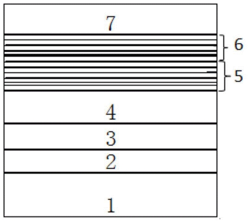
[0046] refer to figure 1 , taking the preparation of an LED structure with a P-type superlattice structure on a silicon carbide substrate by metal-organic chemical vapor deposition as an example, including the following steps:

[0047] (1) The silicon carbide substrate 1 is placed in the reaction chamber of a metal organic chemical vapor deposition furnace (MOCVD), heated to 1250° C. under a hydrogen atmosphere, and processed for 15-20 minutes.

[0048] (2) An aluminum nitride nucleation layer 2 is grown on a silicon carbide substrate 1 at a growth temperature of 750° C., a thickness of 45 nm, and a growth pressure of 50 mbar.

[0049] (3) A non-doped gallium nitride layer (buffer layer) 3 is grown on the aluminum nitride nucleation layer 2 at a growth temperature of 1100° C., a growth thickness of 2 μm, and a growth rate of 1.9 μm / h.

[0050] An N-type gallium nitride layer 4 is grown on the non-doped gallium nitride buffer layer 3 with a thickness of 2 μm. The silicon dopi...

Embodiment 2

[0057] refer to figure 1 , taking the preparation of an LED structure with a P-type superlattice structure on a sapphire substrate by metal-organic chemical vapor deposition as an example, including the following steps:

[0058] (1) The sapphire substrate 1 is put into the reaction chamber of the metal organic chemical vapor deposition furnace (MOCVD), heated to 1000° C. under a hydrogen atmosphere, and processed for 20 minutes.

[0059] (2) An AlGaN nucleation layer 2 is grown on a sapphire substrate 1 at a growth temperature of 560° C., a thickness of 120 nm, and a growth pressure of 500 torr.

[0060] (3) A non-doped GaN layer (buffer layer) 3 is grown on the AlGaN nucleation layer 2 at a growth temperature of 1100° C., a growth thickness of 2 μm, and a growth rate of 2 μm / h.

[0061] N-type gallium nitride 4 is grown on the gallium nitride buffer layer 3, and the silicon doping concentration is 4×10 18 / cm -3 , with a thickness of 2 μm. The growth temperature is about ...

Embodiment 3

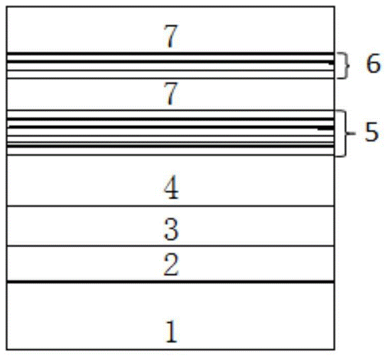
[0068] refer to image 3 , taking the preparation of GaN-based light-emitting diodes containing P-type superlattices on sapphire substrates as an example, the steps are as follows:

[0069] (1) The sapphire substrate 1 is placed in the reaction chamber of a metal organic chemical vapor deposition (MOCVD) furnace, heated to 1000° C. under a hydrogen atmosphere, and processed for 15 minutes.

[0070] (2) Growing gallium nitride nucleation layer 2 on sapphire substrate 1 . The growth temperature is 670° C., and the thickness is 600 nm. The growth pressure was 400 mbar.

[0071] (3) A non-doped gallium nitride layer (buffer layer) 3 is grown on the gallium nitride nucleation layer 2 at a growth temperature of 1050° C., a growth thickness of 1.5 μm, and a growth time of 2100 s.

[0072] N-type gallium nitride 4 is grown on the non-doped gallium nitride buffer layer 3 with a thickness of 3um, and the silicon doping concentration is 3×10 18 / cm -3 , the growth time is 3000s, and...


PUM


Abstract

The invention relates to a GaN-based LED epitaxial structure and a growth method for improving luminous efficiency. In the LED epitaxial structure, there are a nucleation layer, a buffer layer, an n-type GaN layer, a multi-quantum well light-emitting layer, and a P-type structure on the substrate from bottom to top. The P-type structure is composed of an insertion layer and a P-type GaN layer in sequence. Or P-type GaN layer, insertion layer and P-type GaN layer; the insertion layer is a P-type superlattice of LD / PAlXInYGa1-X-YN / HD, LD is a low-doped P-type AlUInNGa1-N-UN layer, and HD is a high Doped P-type AlZInWGa1-Z-WN layer. The present invention uses the P-type superlattice structure, the low-doped LD part prevents P-type impurities from diffusing to the lower light-emitting region, and the high-doped HD part provides a large number of holes; the combination of low-doped and high-doped can provide a large number of holes In this case, the overflow of holes is blocked. At the same time, the P-type AlInGaN layer can effectively trap holes and improve the lateral expansion of holes while blocking electrons. The GaN-based LED with the P-type structure of the invention can significantly improve the quantum efficiency of the device.

Description

technical field [0001] The invention relates to a GaN-based LED epitaxial structure and a growth method for improving luminous efficiency, and belongs to the technical field of optoelectronic chip structures. Background technique [0002] Semiconductor light-emitting diodes have the advantages of small size, ruggedness, strong controllability of light-emitting bands, high luminous efficiency, low heat loss, low light decay, energy saving, and environmental protection. Communication and other fields have a wide range of applications, and gradually become a research hotspot in the field of electronic power. Gallium nitride material has a series of advantages such as wide band gap, high electron mobility, high thermal conductivity, high stability, etc., so it has a wide range of applications and huge market prospects in high-brightness blue light-emitting diodes. The lighting field puts forward higher and higher requirements for LEDs. How to improve the luminous efficiency and...

Claims


Application Information

Patent Timeline
Patent Type & Authority Patents(China)
IPC IPC(8): H01L33/04H01L33/06H01L33/00
CPCH01L33/007H01L33/04H01L33/06H01L33/14H01L33/145H01L33/32
Inventor 逯瑶曲爽王成新张义田龙敬
Owner SHANDONG INSPUR HUAGUANG OPTOELECTRONICS
Why Eureka
Try Eureka