A polysilicon stress sensor and its manufacturing method

A technology of stress sensor and manufacturing method, which is applied in the fields of integrated circuit manufacturing, packaging and measurement, and can solve problems such as TSV damage and inability to reflect the thermal stress status of TSV structures

Active Publication Date: 2016-05-25
SHANGHAI INST OF MICROSYSTEM & INFORMATION TECH CHINESE ACAD OF SCI
View PDF3 Cites 0 Cited by
  • Summary
  • Abstract
  • Description
  • Claims
  • Application Information

AI Technical Summary

Problems solved by technology

At present, the research on the thermal stress distribution inside the TSV structure is mainly through finite element analysis software simulation and section analysis. The finite element analysis is to calculate the through hole by setting the performance parameters of the materials of each layer of the TSV structure in the software and dividing the grid. The stress distribution in each direction is often different from the actual stress distribution, and the cross-section analysis is to measure the stress of the heat treatment process with the test equipment after cutting along the TSV cross-section, which itself causes damage to the TSV, and the analysis of the TSV cross-section structure It does not reflect the thermal stress of the complete TSV structure
There are also reports in the literature that micro-Raman spectrometers are used to analyze the thermal stress distribution on the surface of TSVs. As we all know, the stress of the through-hole structure is mainly concentrated inside the through-holes, and most of the thermal stress on the surface is often released. Only the thermal stress on the surface is analyzed. stress is never enough

Method used


Image

  • A polysilicon stress sensor and its manufacturing method
  • A polysilicon stress sensor and its manufacturing method
  • A polysilicon stress sensor and its manufacturing method

Examples


Embodiment 1

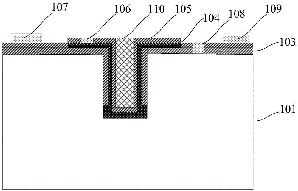
[0057] like figure 2 As shown, this embodiment provides a polysilicon stress sensor, including at least:

[0058] Silicon substrate 101;

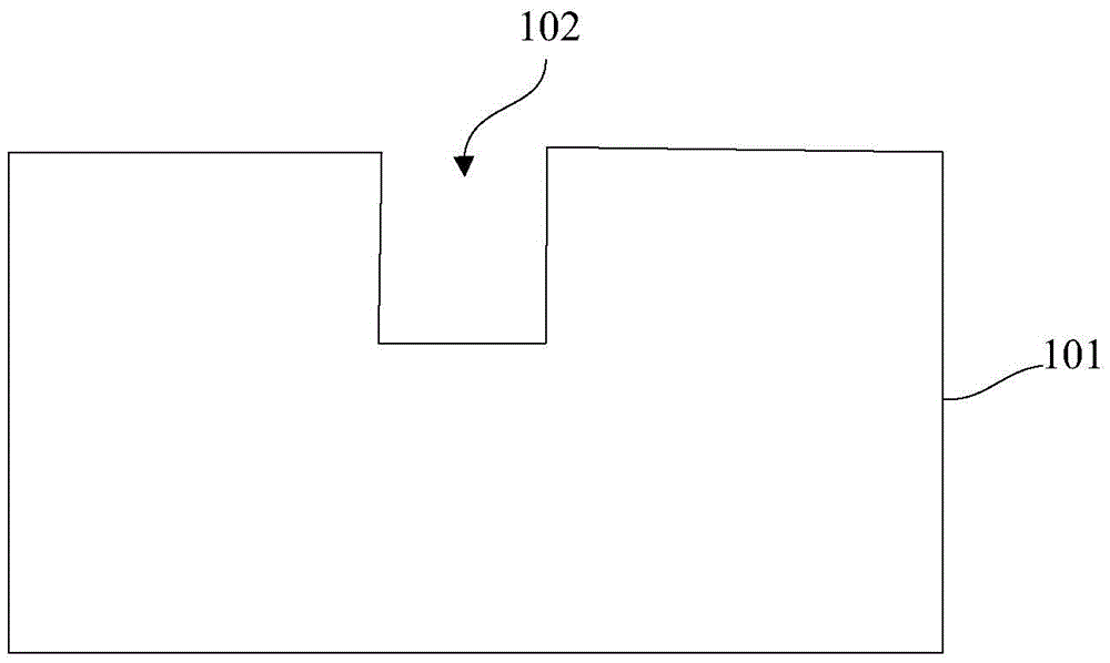
[0059] a silicon hole structure 102 formed in the silicon substrate 101;

[0060] The first barrier layer 103 covers the front surface of the silicon substrate 101 and the upper sidewall of the silicon hole structure 102;

[0061] a polysilicon layer 104 formed on the surface of the first barrier layer 103 and the lower sidewall and bottom of the silicon hole structure 102;

[0062] a second barrier layer 105 covering the surface of the polysilicon layer 104;

[0063] The electrode structure includes a first electrode used to lead out the polysilicon layer 104 and a second electrode used to lead out the silicon substrate 101 .

[0064] The silicon substrate 101 is P-type doped or N-type doped, and the doping concentration is 10 18 ~10 20 / cm 3 , and the doping type of the polysilicon layer 104 is the same as that of the silicon subs...

Embodiment 2

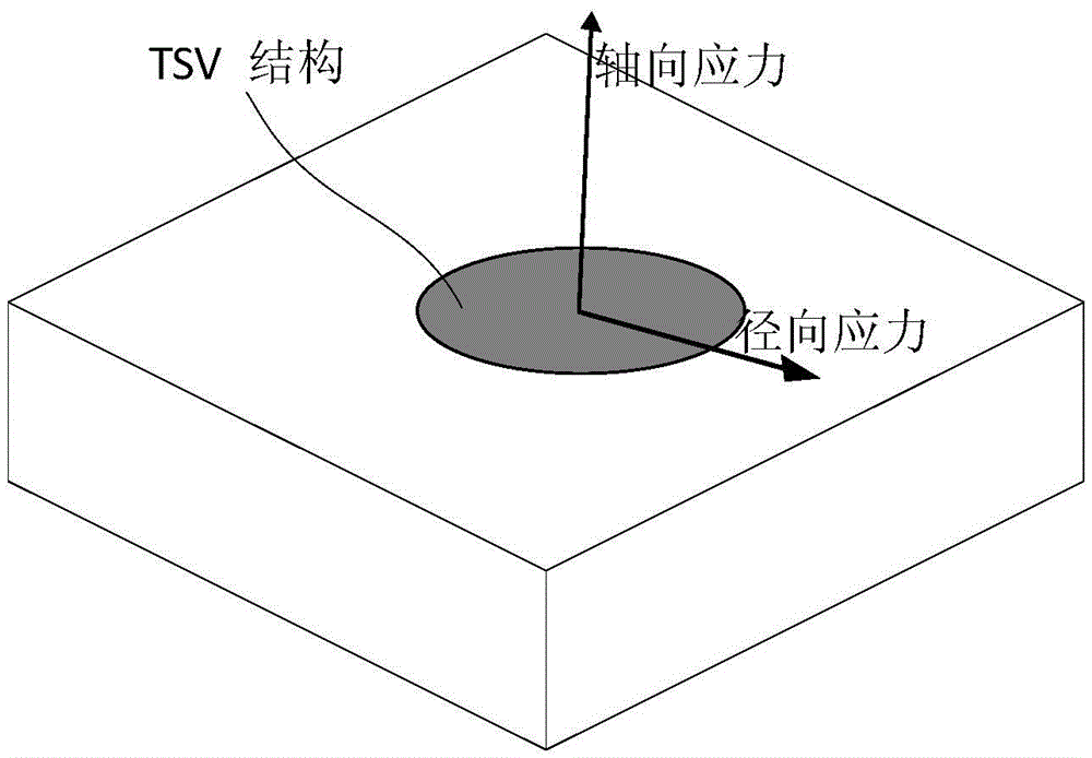
[0087] like Figure 10 As shown, this embodiment provides a method for monitoring the axial stress introduced by electroplating copper-filled silicon hole structure, including the steps: first step, first provide the polysilicon stress sensor as described in embodiment 1, using the conventional needle pressing method, First press the probes on the first pad and the second pad respectively, connect the polysilicon layer (force sensitive resistor) and three additional metal resistors to form a bridge, and test the previous value output of the bridge; In the first step, in the silicon hole structure of the polysilicon stress sensor, after using methods such as electroplating to fill copper 110, then press the probes to the first pad and the second pad, and test the bridge after filling copper 110 By comparing the front value and the back value of the bridge, the axial stress introduced by the silicon hole structure during the copper electroplating process can be obtained by calcu...

Embodiment 3

[0089] like Figure 10 ~ Figure 11 As shown, this embodiment provides a method for monitoring the axial stress generated in the process of thinning the backside of the silicon hole structure to form the through-silicon via, including the steps: the first step, first providing the polysilicon stress sensor as described in Embodiment 1 In the silicon hole structure of the polysilicon stress sensor, copper 110 is filled by electroplating or other methods; in the second step, the probes are respectively pressed onto the first pad and the second pad by using a conventional needle pressing method , connect the polysilicon layer (force-sensitive resistor) with three additional metal resistors to form a bridge, and test the previous value output of the bridge; the third step is to thin the silicon substrate 101 of the polysilicon stress sensor, and pass The HF solution exposes the filled copper 110, and uses the conventional needle pressing method to press the probes onto the first pa...


PUM

PropertyMeasurementUnit
pore sizeaaaaaaaaaa
depthaaaaaaaaaa
thicknessaaaaaaaaaa

Abstract

The invention provides a polysilicon stress sensor and a making method thereof. The polysilicon stress sensor at least includes: a silicon substrate; a silicon pore structure formed in the silicon substrate; a first barrier layer, which covers the front surface of the silicon substrate and the upper side wall of the silicon pore structure; a polysilicon layer, which is formed on the first barrier layer surface, and the lower side wall and bottom of the silicon pore structure; a second barrier layer, which covers the polysilicon layer surface; and an electrode structure, which includes a first electrode for leading out the polysilicon layer and a second electrode for leading out the silicon substrate. According to the invention, a polysilicon force sensing resistor is made on the side wall of a blind hole or through-hole, and by means of the connection effect of the substrate silicon, making of two end leads of the force sensing resistor and a bonding pad on a silicon chip front side can be achieved. At the same time, as the axial force sensitivity of a polysilicon resistor in the hole is far larger than the radial sensitivity, the sensor provided by the invention can be used for measuring the internal axial stress introduced during electroplating copper filling of blind hole and through-hole heat treatment.

Description

technical field [0001] The invention belongs to the technical field of integrated circuit manufacturing, packaging and measurement, and in particular relates to a polysilicon stress sensor and a manufacturing method thereof. Background technique [0002] With the development of three-dimensional packaging and three-dimensional chip stacking technology, Through Silicon Via (TSV) technology has become one of the advanced technologies in the integrated circuit industry. Compared with traditional two-dimensional integration, TSV interconnect technology provides vertical and shorter-distance connections, reduces the distance of information circulation, and improves packaging integration. TSV interconnection has won more and more attention and has been widely used in radio frequency systems, imaging sensors, high-speed logic memory chips, multi-core processors, etc. [0003] Since the TSV structure is a Cu-Si composite structure filled with electroplated copper, the structure has...

Claims


Application Information

Patent Timeline
Patent Type & Authority Patents(China)
IPC IPC(8): B81C1/00G01L1/18
Inventor 豆传国杨恒吴燕红李昕欣
Owner SHANGHAI INST OF MICROSYSTEM & INFORMATION TECH CHINESE ACAD OF SCI
Why Eureka
Try Eureka