A multi-layer film structure electrochromic display
An electrochromic and display technology, applied in instruments, nonlinear optics, optics, etc., can solve the problem of single variable color
- Summary
- Abstract
- Description
- Claims
- Application Information
AI Technical Summary
Problems solved by technology
Method used
Image
Examples
specific Embodiment approach 1
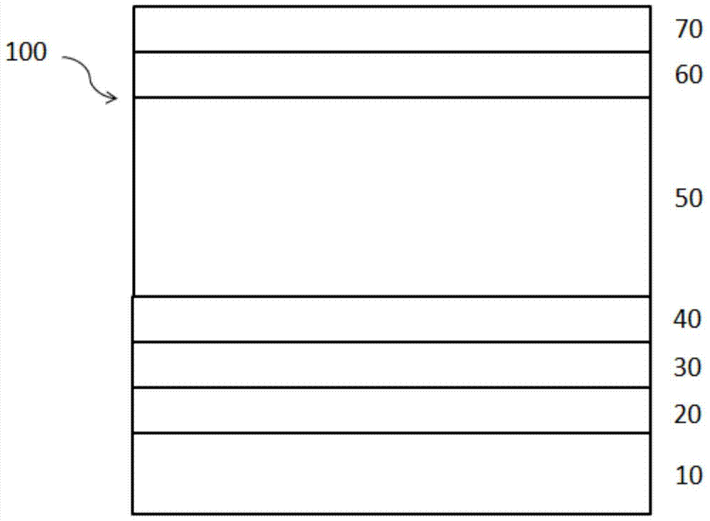
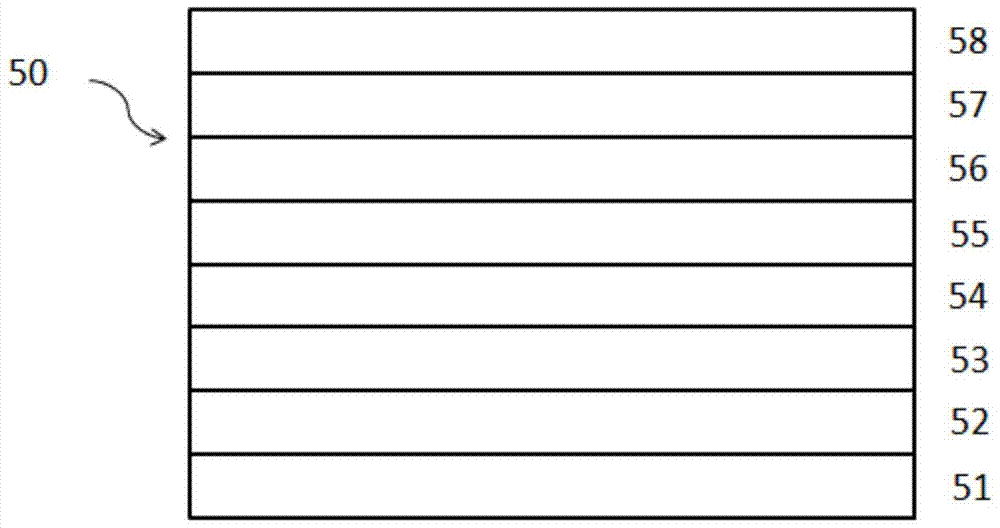
[0020] A multilayer film structure electrochromic display 100, such as figure 1 . Using any material as the substrate 10 , the bottom electrode layer 20 , the ion storage layer 30 , the electrolyte layer 40 , the one-dimensional photonic crystal color changing layer 50 , the top electrode layer 60 and the protective layer 70 are sequentially sputtered by magnetron sputtering.
[0021] The substrate 10 can be any flexible or rigid substrate, which supports the entire display; the bottom electrode layer 20 and the top electrode layer 60 can be the same or different, and are made of transparent metal oxides such as tin-doped indium oxide, fluorine-doped The ion storage layer 30 can be any electrochromic material, such as tungsten oxide, nickel oxide, titanium oxide, molybdenum oxide, vanadium pentoxide, or two of them. or a mixture of many; the electrolyte layer 40 is an electronically insulating and ionically conductive material that must be thick enough to prevent short circui...
specific Embodiment approach 2
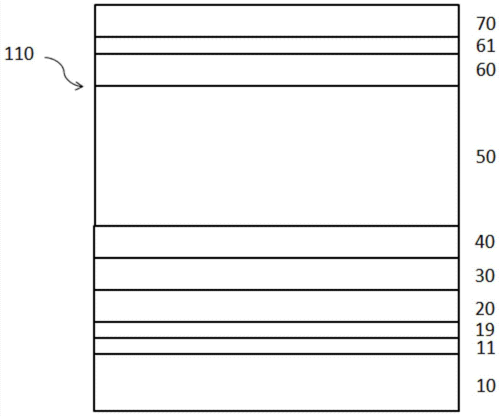
[0023] A multilayer film structure electrochromic display 110, such as image 3 . Taking any material as the substrate 10, the magnetron sputtering method is used to sputter the ion blocking layer 11, the bottom metal electrode layer 19, the bottom electrode layer 20, the ion storage layer 30, the electrolyte layer 40, the one-dimensional photonic crystal color changing layer 50, The top electrode layer 60 , the top metal electrode layer 61 and the protective layer 70 .
[0024] The substrate 10 is a rigid glass substrate, which supports the entire display; the ion blocking layer 11 is generally composed of silicon dioxide to block sodium ions in the glass from entering the device; the bottom metal electrode layer 19 and the top metal electrode layer 61 are made of metal The bottom electrode layer 20 and the top electrode layer 60 can be the same or different, and they are made of transparent metal oxides such as tin-doped indium oxide, fluorine-doped tin oxide, aluminum-dope...
PUM
| Property | Measurement | Unit |
|---|---|---|
| thickness | aaaaa | aaaaa |
| thickness | aaaaa | aaaaa |
| thickness | aaaaa | aaaaa |
Abstract
Description
Claims
Application Information
 - R&D
- Intellectual Property
- Life Sciences
- Materials
- Tech Scout
- Unparalleled Data Quality
- Higher Quality Content
- 60% Fewer Hallucinations
Browse by: Latest US Patents, China's latest patents, Technical Efficacy Thesaurus, Application Domain, Technology Topic, Popular Technical Reports.
© 2025 PatSnap. All rights reserved.Legal|Privacy policy|Modern Slavery Act Transparency Statement|Sitemap|About US| Contact US: help@patsnap.com


