Supercharge Your Innovation With Domain-Expert AI Agents!

A test method for analyzing metal contamination in silicon wafer body

A technology of metal contamination and testing methods, which is applied in semiconductor/solid-state device testing/measurement, material analysis by measuring secondary emissions, optical testing of defects/defects, etc. It can solve the problem of increasing the number of defects, affecting device performance, and channel Incomplete etching and other problems

Active Publication Date: 2017-11-07
GRINM SEMICONDUCTOR MATERIALS CO LTD
View PDF4 Cites 0 Cited by
  • Summary
  • Abstract
  • Description
  • Claims
  • Application Information

AI Technical Summary

Problems solved by technology

When the channel is etched in the device etching process, because these metal silicides will hinder the downward etching of the channel, resulting in incomplete channel etching
Incompletely etched channel morphology will also lead to an increase in the number of defects in subsequent processes, affecting device performance

Method used


Image

  • A test method for analyzing metal contamination in silicon wafer body
  • A test method for analyzing metal contamination in silicon wafer body
  • A test method for analyzing metal contamination in silicon wafer body

Examples


Embodiment 1

[0023] The testing process of metal contamination on the surface of the silicon wafer in this embodiment is:

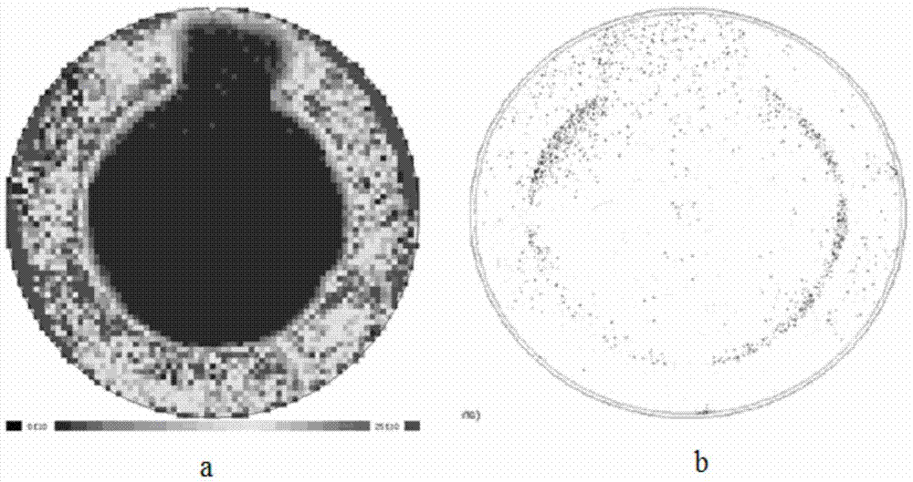
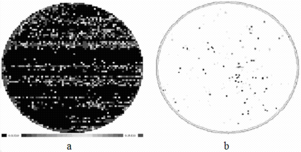
[0024] 1. Silicon wafer selection: Collect the silicon wafers with excessive body iron in the SPV-Fe test and special pattern distribution, and save the SPV-Fe test results of each wafer.

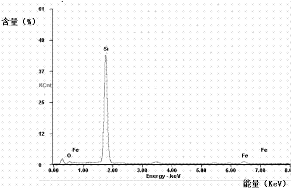
[0025] 2. Wafer cleaning: the silicon wafers with Fe contamination are cleaned in a silicon wafer cleaning machine. The cleaning process is completed in accordance with the standard cleaning procedure: SC-1 cleaning + pure water cleaning + HF cleaning + pure water cleaning + SC- 1 Cleaning + pure water cleaning + SC-2 cleaning + pure water cleaning + drying. After cleaning, use the surface particle tester SP1 to measure the surface particle distribution, and use ICP-MS to analyze the surface metal contamination distribution. After testing, it was found that the amount of surface particle contamination and the amount of metal contamination were both within a controllable range. See Tab...


PUM


Abstract

The present invention provides a kind of test method that is used to analyze the metal contamination in the silicon wafer, comprising the following steps: (1) cleaning the silicon wafer, removing particles and metals on the surface of the silicon wafer, and then loading the silicon wafer into the chamber of an oxidation furnace; 2) Under the mixed atmosphere of high temperature, argon and oxygen, the oxide layer is grown on the surface of the silicon wafer. (4) Use a scanning electron microscope to analyze the particle aggregation area, test the defect components, and make a qualitative judgment on the contamination. In the present invention, an oxide layer is grown on the surface of the silicon wafer during the heat treatment process, so that the metal in the body diffuses to the surface of the silicon wafer, and gathers at the interface of the silicon wafer surface / oxidation layer to form agglomeration of defects, thereby indirectly testing the distribution of metal contamination.

Description

Technical field [0001] The invention relates to a qualitative analysis method of metal in an integrated circuit silicon chip, in particular to a test method for analyzing metal contamination in a silicon chip. Background technique [0002] With the rapid development of integrated circuit technology, the control of metal contamination becomes more and more important in the manufacture of integrated circuits when the line width of lithography is gradually reduced, so the requirements for silicon substrates are also stricter. Metal contamination mainly refers to metals such as Na, Mg, K, Al, Ca, Zn, Fe, Cu, Ni, Co, etc. According to the location of the contamination, it can be divided into surface contamination and internal contamination: surface contamination is mainly in silicon Wafers are formed during mechanochemical processing, mainly in the processes of silicon wafer cutting, grinding, polishing, transfer and transportation; while bulk metal contamination is mainly formed in t...

Claims


Application Information

Patent Timeline
Patent Type & Authority Patents(China)
IPC IPC(8): H01L21/66G01N21/88G01N23/22
Inventor 冯泉林闫志瑞赵而敬李宗峰盛方毓程凤伶孙媛
Owner GRINM SEMICONDUCTOR MATERIALS CO LTD
Features
  • R&D
  • Intellectual Property
  • Life Sciences
  • Materials
  • Tech Scout
  • Unparalleled Data Quality
  • Higher Quality Content
  • 60% Fewer Hallucinations
Learn More