Semiconductor light-emitting device and manufacturing method thereof

A technology for light-emitting devices and semiconductors, which is applied to semiconductor devices, electrical components, circuits, etc., and can solve the problems of less quantum well polarization charge, weakened quantum well tilt, and low growth temperature.

Active Publication Date: 2015-06-24
扬州德豪润达光电有限公司
View PDF11 Cites 14 Cited by
  • Summary
  • Abstract
  • Description
  • Claims
  • Application Information

AI Technical Summary

Problems solved by technology

The Chinese invention patent application with publication number 102449737A discloses a method for growing III-nitride thin films on non-polar or semi-polar surfaces to reduce the polarization charges in quantum wells; but in this method, The quantum wells in the non-polar or semi-polar plane have very few polarized charges, the polarization field is small, and the quantum well energy band tilt is weakened. Therefore, to achieve the same wavelength, more In components need to be contained, while in The incorporation efficiency of In components on the nonpolar and semipolar surfaces is low, requiring lower growth temperatures, which will deteriorate the crystal quality of quantum wells

Method used


Image

  • Semiconductor light-emitting device and manufacturing method thereof
  • Semiconductor light-emitting device and manufacturing method thereof
  • Semiconductor light-emitting device and manufacturing method thereof

Examples


Embodiment Construction

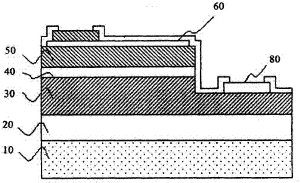
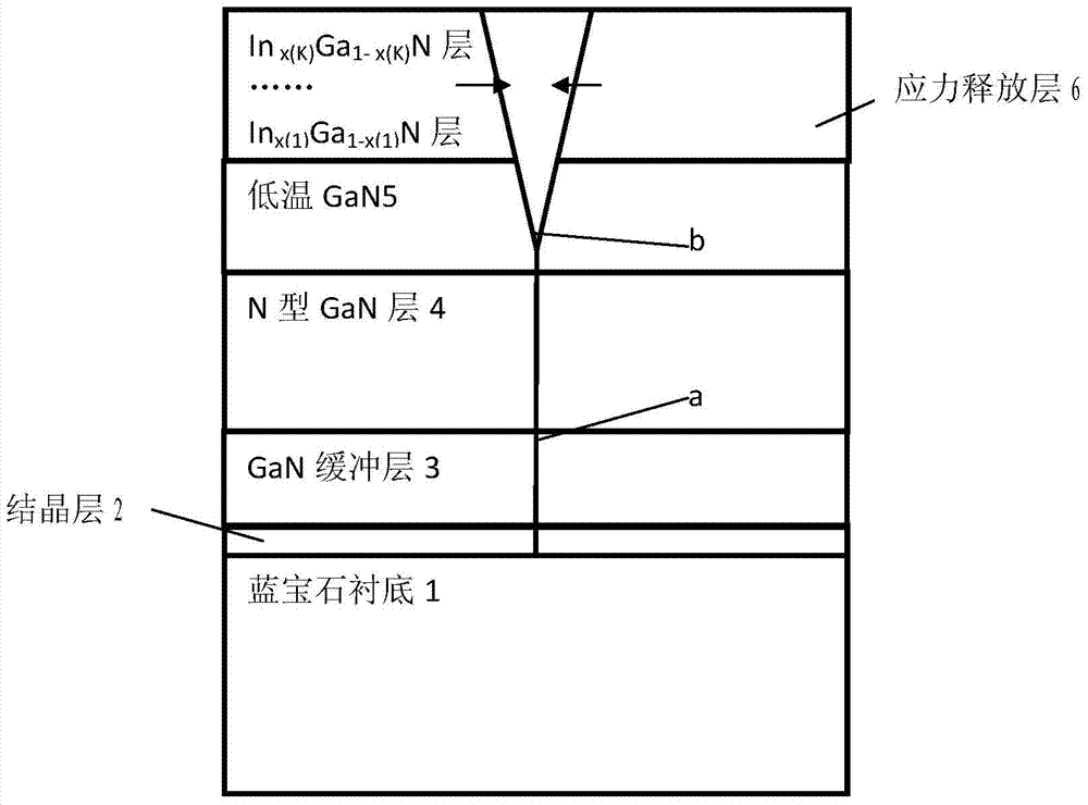
[0033] The semiconductor light-emitting device of the present invention comprises a substrate, a crystalline layer sequentially formed on the substrate, a gallium nitride buffer layer, an N-type gallium nitride layer, a low-temperature gallium nitride layer, a stress release layer, a transition layer, and a multi-quantum well layer and the P-type gallium nitride layer, the N electrode and the P electrode respectively form ohmic contacts with the N-type gallium nitride layer and the P-type gallium nitride layer through a micro-alloy process. The substrate of the present invention can be a commonly used substrate for the growth of gallium nitride epitaxial materials such as sapphire, silicon carbide, silicon, and homogeneous gallium nitride. The crystallization layer, the gallium nitride buffer layer, and the n-type gallium nitride layer are grown and formed using traditional process conditions.

[0034]In the invention, a low-temperature gallium nitride layer is grown on the N-...


PUM

PropertyMeasurementUnit
thicknessaaaaaaaaaa
thicknessaaaaaaaaaa
thicknessaaaaaaaaaa

Abstract

The invention discloses a semiconductor light-emitting device and a manufacturing method thereof. The semiconductor light-emitting device comprises a substrate, a crystallizing layer formed on the substrate, a gallium nitride buffering layer, an N-type gallium nitride layer, a transition layer, a multi-quantum-well layer and a P-type gallium nitride layer and further comprises a low-temperature gallium nitride layer and a stress release layer, wherein the low-temperature gallium nitride layer is formed on the N-type gallium nitride layer, a plurality of concave pits are formed in the low-temperature gallium nitride layer, the thickness of the stress release layer is smaller than 100 nm, the stress release layer is composed of 1-K layers of Inx(k)Ga1- x(K)N which are sequentially formed on the low-temperature gallium nitride layer, the thickness d<k> of the kth layer of Inx(k)Ga1- x(K)N is smaller than the thickness d<k-1> of the (k-1)th layer of Inx(k-1)Ga1- x(K-1)N, x(k) is larger than x(k-1), k is equal to 1,...,K, and K is smaller than or equal to 5; the concave pits are covered with the P-type gallium nitride layer. The number of the InGaN layers in the stress release layer and the overall thickness are adjusted according to In components of quantum wells so that the In components of the InGaN layers can be gradually increased from the bottom layer to the surface, the thickness is gradually reduced, and the purpose of gradually releasing stress is achieved.

Description

technical field [0001] The invention belongs to the technical field of semiconductor light emitting devices, and in particular relates to a Group III nitride semiconductor device and a preparation method thereof. Background technique [0002] The emergence of semiconductor light-emitting devices has brought light sources that can cover the visible spectrum and have higher luminous efficiency and solid-state stability. Semiconductor light emitting devices, such as light emitting diodes (LEDs) or laser diodes, have been widely used in many fields. Light emitting diodes or laser diodes generally comprise nitride semiconductor layers fabricated by epitaxial processes on a microelectronic substrate, which may be gallium arsenide, gallium phosphide, silicon carbide and / or sapphire, and on the substrate. Visible light-emitting diodes based on group III nitride semiconductors have been widely used in the fields of indoor and outdoor color display, backlight and lighting in recent y...

Claims


Application Information

Patent Timeline
Patent Type & Authority Applications(China)
IPC IPC(8): H01L33/12H01L33/32H01L33/00
Inventor 王冬雷梅劲陈刚毅
Owner 扬州德豪润达光电有限公司
Why Eureka
Try Eureka