Solar cell
A technology of solar cells and sub-cells, which is applied in the field of photoelectric components and solar cells, can solve the problems of inefficient regulation, degradation of battery performance, and inability to achieve high n-type doping concentration, so as to reduce lateral expansion resistance and increase current carrying Sub-lifetime, the effect of reducing interfacial recombination
- Summary
- Abstract
- Description
- Claims
- Application Information
AI Technical Summary
Problems solved by technology
Method used
Image
Examples
Embodiment 1
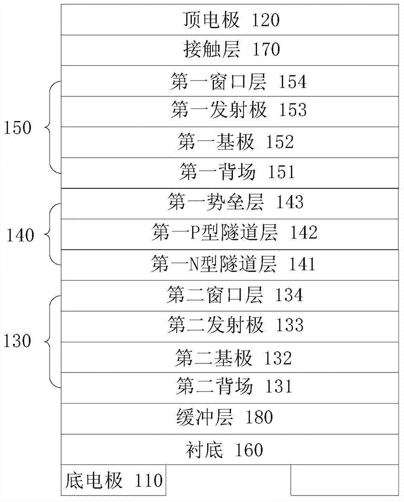
[0025] refer to figure 1 , is a schematic diagram of the solar structure provided in this embodiment, the solar cell includes a bottom electrode 110, a substrate 160, a second sub-cell 130, a first tunnel junction 140, a first sub-cell 150, and a contact layer arranged in sequence from bottom to top 170 and the top electrode 120, wherein the energy band system of the second sub-cell is smaller than that of the first sub-cell, and the lattice constant of the first sub-cell 150 is matched with the GaAs lattice. In this embodiment, we take the first sub-cell 150 made of GaInP material as an example for illustration. Of course, in other embodiments, the first sub-cell may also be a GaAs solar cell.
[0026] In this embodiment, the material of the substrate 160 is P-type doped GaAs, wherein the P-type dopant source is Be. In order to improve the growth quality of the second sub-cell 130 , a buffer layer 180 is provided on the substrate 160 , and the material of the buffer layer 18...
Embodiment 2
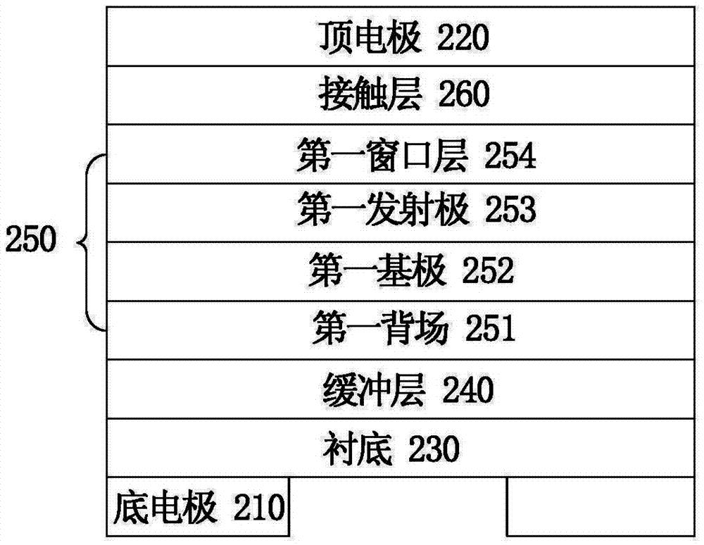
[0031] refer to figure 2 , is a schematic diagram of the solar structure provided in this embodiment, the solar cell includes a bottom electrode 210, a substrate 230, a buffer layer 240, a first sub-cell 250, a contact layer 260, and a top electrode 220 arranged sequentially from bottom to top, wherein, The lattice constant of the first sub-cell 250 is matched with the GaAs lattice. In this embodiment, we take the first sub-cell 250 of GaInP material as an example for illustration. Of course, in other embodiments, the first sub-cell 250 can also choose GaAs solar cells.
[0032]In this embodiment, the material of the substrate 230 is P-type doped GaAs, wherein the P-type dopant source is Be. In order to improve the growth quality of the first sub-cell 250 , a buffer layer 240 is provided on the substrate 230 , and the material of the buffer layer 240 is P-type GaAs.
[0033] Further, the first sub-cell 250 includes a first back field 251 , a first base 252 , a first emitter...
PUM
 Abstract
Description
Claims
Application Information

