Method for manufacturing semiconductor chips and surface protective tape for thin-film grinding used in same

A manufacturing method and semiconductor technology, which can be used in the manufacture of semiconductor/solid-state devices, semiconductor devices, film/sheet adhesives, etc. The effect of precision and simple manufacturing methods

Inactive Publication Date: 2015-07-15
FURUKAWA ELECTRIC CO LTD
View PDF11 Cites 22 Cited by
  • Summary
  • Abstract
  • Description
  • Claims
  • Application Information

AI Technical Summary

Problems solved by technology

However, the peeling force from the adhesive tape tends to increase by heating and bonding, and there is a problem that it is difficult to peel from the adhesive tape after heating and bonding.
[0013] These problems have also been studied (refer to Patent Documents 8 and 9), but along with thinning and large-diameter in recent years, inconveniences such as cracks are likely to occur in conventional semiconductor chip manufacturing methods, and in the worst case, The problem of poor yield due to wafer cracking
Especially in the polishing of wafers with a thickness of 100 μm or less, the deterioration of the yield rate is particularly serious, and it may be difficult to manufacture stably
In addition, it is difficult to improve the flexural strength in chipping by normal back grinding and dicing, and failures in packaging often occur.

Method used


Image

  • Method for manufacturing semiconductor chips and surface protective tape for thin-film grinding used in same
  • Method for manufacturing semiconductor chips and surface protective tape for thin-film grinding used in same
  • Method for manufacturing semiconductor chips and surface protective tape for thin-film grinding used in same

Examples


Embodiment 1

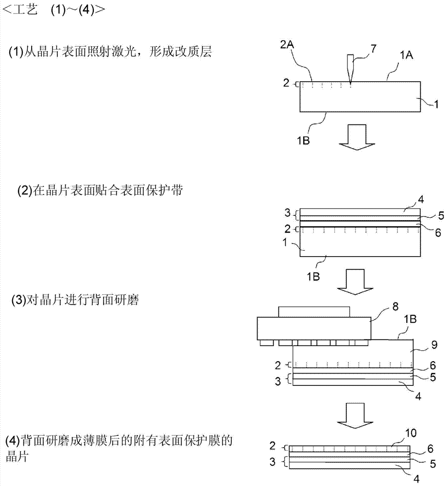
[0251] (I) Fabrication of Surface Protection Tape for Thin Film Polishing

[0252] An ultraviolet curable (meth)acrylic adhesive layer is provided on a substrate film made of ethylene-acrylic acid copolymer with a thickness of 100 μm, and a (meth)acrylic copolymer containing epoxy resin is placed on the adhesive layer. An adhesive layer composed of a substance was used to produce the surface protection tape for film polishing of the present invention.

[0253] (1) Manufacturing method of adhesive tape

[0254] Blend 78 mol% of 2-ethylhexyl acrylate, 21 mol% of 2-hydroxyethyl acrylate, and 1 mol% of methacrylic acid, and copolymerize them in an ethyl acetate solution to obtain a copolymer solution with a weight average molecular weight of 700,000 . With respect to 100 parts by mass of the copolymer, 5.0 parts by mass of 2-methacryloyloxyethyl isocyanate (trade name, Karenz MOI manufactured by Showa Denko Co., Ltd.) was mixed in the solution, and they were mixed in the solutio...

Embodiment 2

[0276] Using the surface protection tape for film polishing made in Example 1, the process of (6) in Example 1 is changed to the process of the following (6-1) to (6-2), and in addition, A semiconductor chip was produced in the same manner as in Example 1.

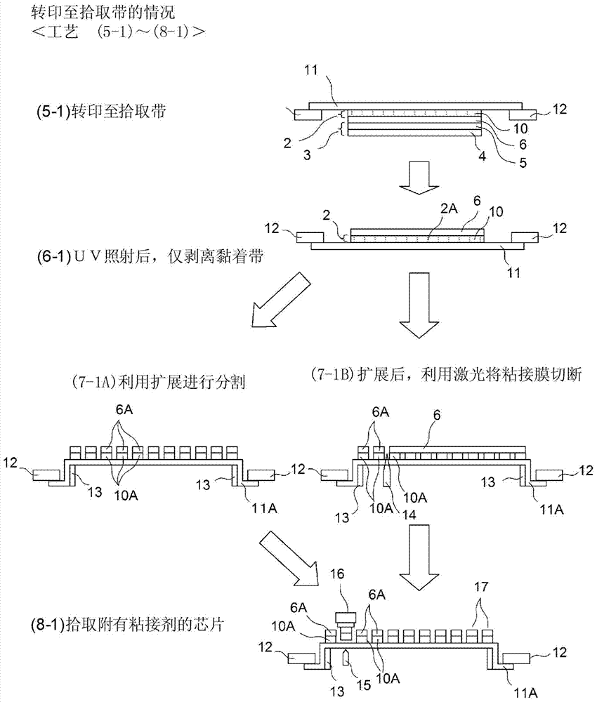
[0277] (6-1) The pick-up tape (11) was expanded under conditions of a speed of 1 mm / sec and an expansion amount of 8 mm so as to divide only the semiconductor wafer.

[0278] (6-2) After the above expansion, the adhesive film (adhesive layer) (6) is cut with a laser ( 14 ). { figure 2 Process shown in (7-1B)}

Embodiment 3

[0280] by figure 1 and image 3 The process of making semiconductor chips.

[0281] Use the surface protection tape for film polishing that is made in embodiment 1, after carrying out the process of (1)~(3) in embodiment 1, carry out following process (4A)~(6A) instead of (4)~( 7), Manufacturing semiconductor chips.

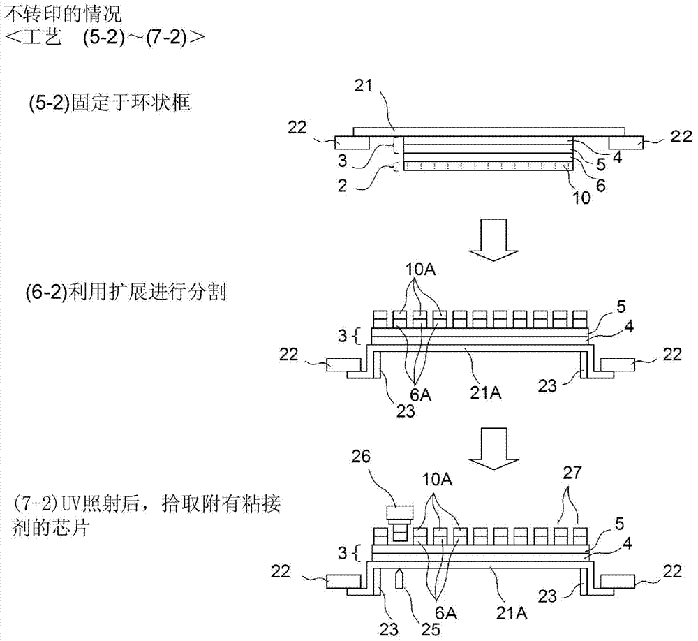
[0282] (4A) Attach the same expansion tape (11) (fixation tape (21)) as in Example 1 to the base film (4) side of the film polishing surface protection tape, and fix it to the ring frame (22) . The expanding tape (11) (fixing tape (21)) has an adhesive layer made of an ultraviolet-curable acrylic copolymer on a base film made of vinyl ionomer resin.

[0283] (5A) Expand the above-mentioned fixing tape (21) at a speed of 1 mm / sec and an expansion amount of 20 mm, and divide the adhesive film (adhesive layer) (6) from the semiconductor wafer on the adhesive film (3). .

[0284] (6A) The divided semiconductor wafer (10A) becomes each chip (27) with an adhesive...


PUM


Abstract

[Problem] To provide a high precision and simple method for manufacturing semiconductor chips in semiconductor chip manufacturing that carries out back surface grinding of a semiconductor wafer which is used in a flip chip mounting process and has bump electrodes and simultaneously or in a process thereafter carries out chip formation without using underfilling, and also to provide a surface protective tape for thin-film grinding used in that method. [Solution] This manufacturing method for semiconductor chips grinds the back surface of a semiconductor wafer after formation of a modified layer within a wafer with bump electrodes, which has bumps for electrodes, on the semiconductor wafer on which a semiconductor circuit has been formed, and carries out division into individual chips in a batch. This method for manufacturing semiconductor chips has a step for applying surface protective tape for thin-film grinding in which a bonding film is laminated on an adhesive layer in an adhesive tape that has an adhesive layer on a base material film to the side of a semiconductor wafer on which a semiconductor circuit is formed on the bonding film side after formation of the modified layer and before the back surface of the semiconductor wafer is ground, and a step for creating a state in which only the bonding film bonds to the chips when the chips are picked up after back surface grinding of the semiconductor wafer or when transferred to a tape used for pick-up. The surface protective tape for thin-film grinding used therein is also provided.

Description

【Technical field】 [0001] The present invention relates to a method for manufacturing a semiconductor chip and a surface protection tape for thin film polishing used in the method. 【Background technique】 [0002] In recent years, the spread of IC cards and the rapid increase in the capacity of USB memory have been progressing, and further thinning is expected along with the increase in the number of stacked chips. Therefore, it is necessary to reduce the thickness of the semiconductor chip from about 200 μm to 350 μm to a thickness of 50 to 100 μm or less. As a method for achieving such a thinning of the chip, there are known a method of using a special tape and performing thinning and polishing in a normal process, or a manufacturing method called dicing first (that is, forming a chip at a predetermined depth from the wafer surface side). A method of manufacturing a semiconductor chip that is ground from the back side after the groove). This method can efficiently manufact...

Claims


Application Information

Patent Timeline
Patent Type & Authority Applications(China)
IPC IPC(8): H01L21/301H01L21/304
CPCH01L2221/68381C09J1/00H01L2221/68336H01L21/6836H01L2221/68377H01L2221/68327H01L2221/6834C09J7/243C09J7/385C09J2203/326
Inventor 横井启时冈祥文青山真沙美
Owner FURUKAWA ELECTRIC CO LTD
Why Eureka
Try Eureka