Gete/sb type superlattice phase change thin film material for high-speed phase change memory and preparation method thereof

A phase-change memory and thin-film material technology, which is applied in metal material coating technology, ion implantation plating, coating, etc., can solve the problems of unfavorable memory, slowing down of phase change speed, and slowing down the crystallization speed of materials, so as to reduce heat loss. Conductivity, inhibition of crystallization, and effect of grain size reduction

Inactive Publication Date: 2018-04-13
JIANGSU UNIV OF TECH
View PDF9 Cites 3 Cited by
  • Summary
  • Abstract
  • Description
  • Claims
  • Application Information

AI Technical Summary

Problems solved by technology

However, the phase change material disclosed in this patent document improves the Ge 2 Sb 2 Te 5 Thermal stability will inevitably slow down the crystallization rate of the material, so that Ge 2 Sb 2 Te 5 The inherently slow phase transition speed is further reduced, which is very unfavorable for the application of memory

Method used


Image

  • Gete/sb type superlattice phase change thin film material for high-speed phase change memory and preparation method thereof
  • Gete/sb type superlattice phase change thin film material for high-speed phase change memory and preparation method thereof

Examples


Embodiment 1)

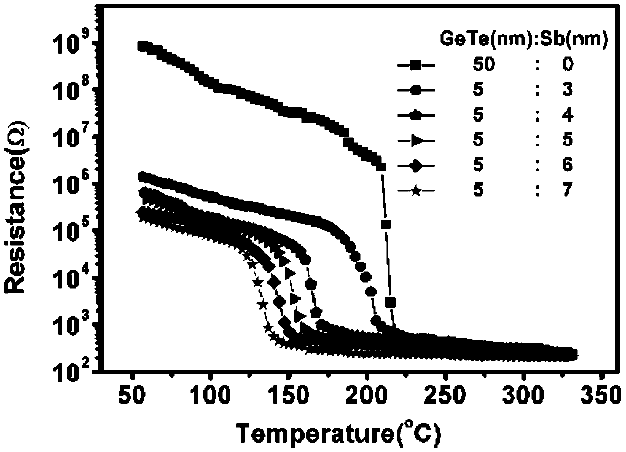
[0030]The GeTe / Sb superlattice phase change thin film material used in the high phase change memory of this embodiment is a multilayer composite film structure with a thickness of 6-80nm; it is composed of GeTe layers and Sb layers alternately deposited, that is, in the thin film Among them, the GeTe layer-Sb layer-GeTe layer-Sb layer... order is repeated and alternately arranged.

[0031] A GeTe layer and a Sb layer are used as an alternating cycle, and the GeTe layer of the latter alternate cycle is deposited on the Sb layer of the previous alternate cycle. The GeTe layer contains two elements, Ge and Te, and the atomic ratio of Ge and Te is 1:1.

[0032] The general formula [GeTe (a) / Sb (b)] for the film structure of above-mentioned Ge Te / Sb class superlattice phase change film material x where a is the thickness of the single-layer GeTe layer, 1nm≤a≤50nm; b is the thickness of the single-layer Sb layer, 1nm≤b≤50nm; x is the number of alternating periods of the GeTe layer ...

Embodiment 2)

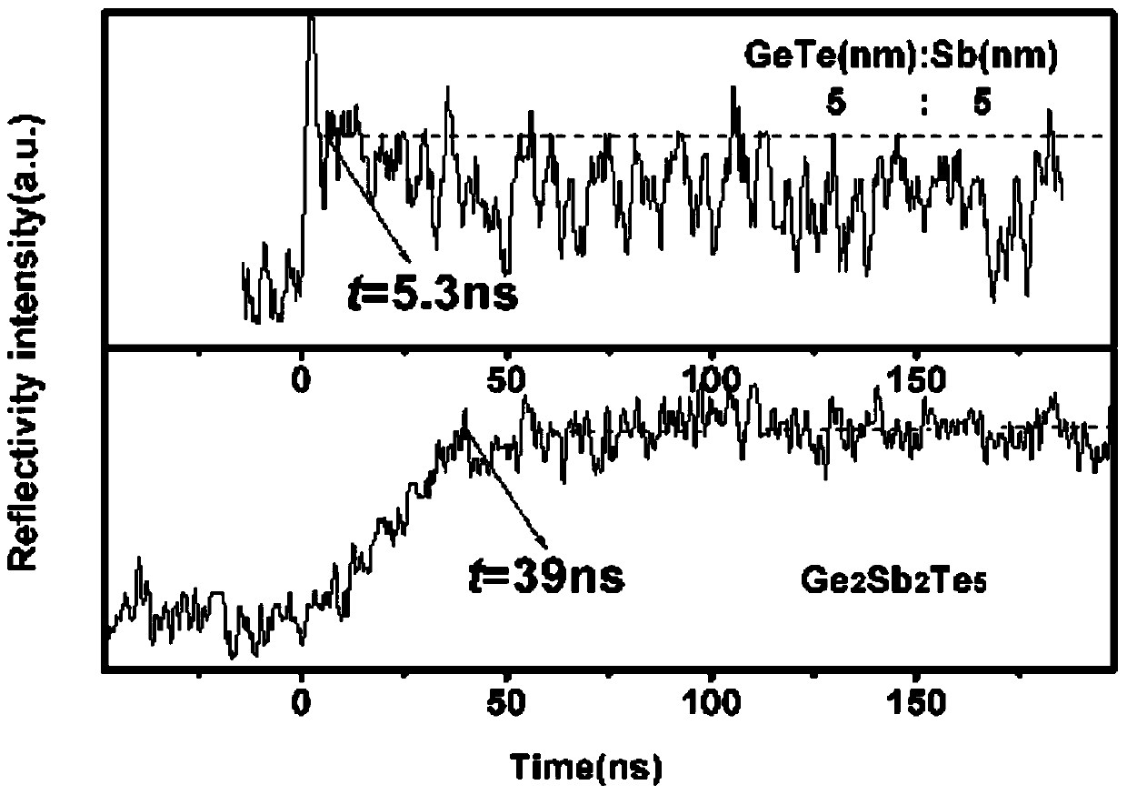
[0046] The film structure of the GeTe / Sb class superlattice phase change film material used for high phase change memory of the present embodiment is [GeTe (5nm) / Sb (4nm)] 6 , that is, the thickness of each layer of GeTe layer is 5nm, the thickness of each layer of Sb layer is 4nm, the number of alternating periods of GeTe layer and Sb layer is 6, and the thickness of GeSb superlattice phase change thin film material is 54nm.

[0047] The rest of the preparation method is the same as that of Example 1, except that: Step ③ When preparing GeTe / Sb superlattice phase change thin film material by magnetron sputtering, the sputtering time of each layer of Sb is 16s.

Embodiment 3)

[0049] The film structure of the GeTe / Sb class superlattice phase change film material used for high phase change memory of the present embodiment is [GeTe (5nm) / Sb (5nm)] 5 , that is, the thickness of each layer of GeTe layer is 5nm, the thickness of each layer of Sb layer is 5nm, the number of alternating cycles of GeTe layer and Sb layer is 5, and the thickness of GeSb superlattice phase change thin film material is 50nm.

[0050] The rest of the preparation method is the same as that of Example 1, except that: Step 3. When preparing GeTe / Sb superlattice phase change thin film material by magnetron sputtering, the sputtering time of each layer of Sb is 20s.


PUM

PropertyMeasurementUnit
thicknessaaaaaaaaaa
thicknessaaaaaaaaaa
thicknessaaaaaaaaaa

Abstract

The invention discloses a GeTe / Sb superlattice phase change thin film material used for high-speed phase change memory. A layer of Sb is used as an alternating period, and the GeTe layer of the latter alternating period is deposited on the Sb layer of the previous alternating period. Tests have proved that the time for the sudden change in the reflectivity of the GeTe / Sb class superlattice phase-change thin film material of the present invention is about 5.3ns, and the time for the sudden change in the reflectivity of the single-layer Ge2Sb2Te5 traditional phase-change thin film material is about 39ns; Compared with the traditional single-layer Ge2Sb2Te5 phase-change thin-film material, the phase-change thin-film material of the present invention has a faster phase-change speed, thereby making the phase-change memory prepared with it have a faster operating speed, which is conducive to improving the read and write performance of PCRAM information. speed.

Description

technical field [0001] The invention relates to a phase-change thin film material in the field of microelectronics, in particular to a GeTe / Sb superlattice phase-change thin film material used for a high-speed phase-change memory and a preparation method thereof. Background technique [0002] Phase-change memory (PCRAM) is a new type of non-volatile memory that uses the huge resistance difference between the crystalline and amorphous states of materials to store information. When the phase change material has a higher resistance in the amorphous state and a lower resistance in the crystalline state, the resistance difference between the two states reaches more than 2 orders of magnitude. The rapid transition of phase-change materials between two resistive states can be achieved through current-induced Joule heating. PCRAM has the advantages of strong stability, low power consumption, high storage density, and compatibility with traditional CMOS processes, so it has attracte...

Claims


Application Information

Patent Timeline
Patent Type & Authority Patents(China)
IPC IPC(8): H01L45/00C23C14/35C23C14/18
Inventor 胡益丰潘佳浩吴小丽朱小芹吴世臣邹华袁丽吴卫华张建豪眭永兴
Owner JIANGSU UNIV OF TECH
Why Eureka
Try Eureka