A MEMS microphone and a formation method thereof

A microphone and substrate technology, applied in the field of MEMS microphone and its formation, can solve the problems of CMOS circuit manufacturing obstacles, increased manufacturing cost, complicated circuit and microphone structure and process, etc.

Active Publication Date: 2015-07-22
MEMSEN ELECTRONICS
View PDF5 Cites 11 Cited by
  • Summary
  • Abstract
  • Description
  • Claims
  • Application Information

AI Technical Summary

Problems solved by technology

[0005] In the existing MEMS microphone manufacturing method, the process of integrating the microphone chip and the CMOS circuit process is quite different, and it is difficult to achieve monolithic integration.
At the same time, when a CMOS circuit and a microphone structure are fabricated on a single substrate, the existence of the microphone structure hinders the manufacture of the CMOS circuit, and the existence of the CMOS circuit on the same substrate also causes difficulties in the manufacture of small-sized microphone structures.
Therefore, the manufacturing process of using a single substrate as a CMOS circuit and a microphone structure is more complicated, and the size of the formed device is larger, resulting in an increase in manufacturing cost.
[0006] When making an integrated microphone structure and CMOS circuit on a single substrate, if the parts of the microphone structure are made first, and then the CMOS circuit is made, the process of manufacturing the microphone structure often affects the substrate, resulting in the difficulty of CMOS circuit production. reduce
If the CMOS circuit is made first, and then the microphone structure is made, the existence of the CMOS circuit has great restrictions on the material selection and process temperature of the microphone structure, thereby seriously reducing the performance of the microphone structure.

Method used


Image

  • A MEMS microphone and a formation method thereof
  • A MEMS microphone and a formation method thereof
  • A MEMS microphone and a formation method thereof

Examples


Embodiment 1

[0106] Figure 1 to Figure 9 It is a schematic cross-sectional structure diagram of the forming process of the MEMS microphone of the embodiment of the present invention.

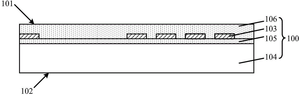
[0107] Please refer to figure 1 , providing a first substrate 100, the first substrate 100 includes an opposite first surface 101 and a second surface 102, the first substrate 100 includes at least one conductive layer 103, and the conductive layer 103 is located at the The side of the first surface 101 of the first substrate 100 described above.

[0108] The first substrate 100 is used to form a conductive layer 103, and the conductive layer 103 is used to transmit electrical signals output by the sensitive electrodes.

[0109] In this embodiment, the first substrate 100 includes a first substrate 104, a first dielectric layer 105 located on the surface of the first substrate 104, and a conductive layer 103 located on the surface of the first dielectric layer 105; the first substrate 100 It also includ...

Embodiment 2

[0192] Figure 11 to Figure 12 is a schematic cross-sectional structure diagram of the forming process of the MEMS microphone according to another embodiment of the present invention.

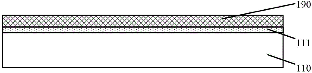
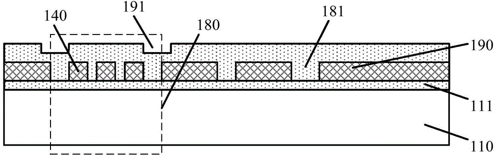
[0193] Please refer to Figure 11 , providing a first substrate 200, the first substrate 200 includes an opposite first surface 201 and a second surface 202, the first substrate 200 includes at least one conductive layer 203, and the conductive layer 203 is located at the On the side of the first surface 201 of the first substrate 200 , the first substrate 200 further includes a self-test electrode 230 .

[0194] In an embodiment, the first substrate 200 further includes a circuit, and the circuit includes a semiconductor device structure and an electrical interconnection structure, and the conductive layer 203 may be a part of the conductive layer of the circuit, or may be on the circuit additional conductive layer. The conductive layer may include a conductor or a semiconductor.

[0195] ...

Embodiment 3

[0224] Figure 13 to Figure 14 is a schematic cross-sectional structure diagram of the forming process of the MEMS microphone according to another embodiment of the present invention.

[0225] Please refer to Figure 13 , providing a second substrate 314, the second substrate 314 includes an opposite third surface 318 and a fourth surface 319, the second substrate 314 includes a second base 310 and a sensitive electrode located on the second base 310 313 , the second substrate 314 includes a sensitive region 380 , the sensitive electrode 313 is located in the sensitive region 380 , and the sensitive electrode 313 is located on the third surface 318 side of the second substrate 314 .

[0226] In this embodiment, it also includes: forming a material layer 383 on the third surface 318 side of the second substrate 314; the second substrate 314 also includes a first electrode layer 312 on the second base 310, the The first electrode layer 312 includes the sensitive electrode 313 ...


PUM


Abstract

Provided are a MEMS microphone and a formation method thereof. The formation method comprises: providing a first substrate comprising a first surface and a second surface, wherein, the first substrate comprises at least one conductive layer, which is located at a side of the first surface of the first substrate; providing a second substrate comprising a third surface and a fourth surface, wherein, the second substrate comprises a second base and a sensitive electrode, and comprises a sensitive area, in which the sensitive electrode is located at a side of the third surface of the second substrate; fixing the first surface of the fist substrate and the third surface of the second substrate each other; thereafter, removing the second base, and forming a fifth surface opposite to the third surface of the second substrate; forming an empty cavity between the first substrate and the sensitive area of the second substrate; and forming, from a side of the fifth surface of the second substate, a first conductive plug penetrating to the at least one conductive layer. The MEMS microphone is improved in performance and reliability, is reduced in size, and is lowed in process cost.

Description

technical field [0001] The invention relates to the technical field of semiconductor manufacturing, in particular to a MEMS microphone and a forming method thereof. Background technique [0002] In recent years, with the rapid development of semiconductor technology, electronic products tend to be designed in the direction of miniaturization and thinning. Among the products in the field of electroacoustics, microphones are used to convert sound waves into electrical signals, and many electronic products currently available on the market are equipped with MEMS (micro-electromechanical) microphones. Compared with common electret microphones (ECM), MEMS microphones are more resistant to heat, vibration, and radio frequency interference. [0003] MEMS microphones are miniature microphones made by etching pressure-sensing diaphragms on semiconductors through micro-electro-mechanical systems technology. They are commonly used in mobile phones, earphones, laptops, cameras and cars...

Claims


Application Information

Patent Timeline
Patent Type & Authority Applications(China)
IPC IPC(8): H04R19/04H04R31/00
CPCH04R19/005B81B3/0021B81B2201/0257B81C1/00238B81C2203/0792H04R19/04H04R23/006H04R31/006H04R2201/003
Inventor 周文卿
Owner MEMSEN ELECTRONICS
Why Eureka
Try Eureka