Misunderstanding prevention resistance random access memory and production method thereof

A resistive variable memory and resistive variable technology, applied in the field of memory, can solve problems such as instability and easy misreading, and achieve the effects of excellent anti-fatigue characteristics, stable resistance changes, and significant switching effects

Active Publication Date: 2015-07-29
HEBEI UNIVERSITY
View PDF3 Cites 8 Cited by
  • Summary
  • Abstract
  • Description
  • Claims
  • Application Information

AI Technical Summary

Problems solved by technology

[0005] One of the purposes of the present invention is to provide a resistive variable memory that avoids misreading, so as to solve the pro

Method used


Image

  • Misunderstanding prevention resistance random access memory and production method thereof
  • Misunderstanding prevention resistance random access memory and production method thereof
  • Misunderstanding prevention resistance random access memory and production method thereof

Examples


Embodiment 1

[0030] Embodiment 1, a resistive memory that avoids misreading.

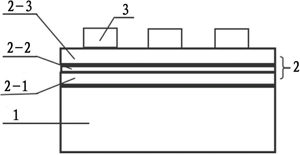
[0031] Such as figure 1 As shown, the anti-misreading resistive memory provided by the present invention has a structure including a substrate 1 at the bottom, a resistive dielectric layer 2 on the substrate 1 and an electrode film layer 3 on the resistive dielectric layer 2 . Substrate 1 is Pt / Ti / SiO 2 / Si substrate, “Pt / Ti / SiO 2 / Si" means that the bottom is Si, Si is SiO 2 , SiO 2 Ti is above Ti, and Pt is above Ti. Therefore, the Pt film layer is the topmost layer of the substrate 1 , and the resistive variable medium layer 2 is located on the Pt film layer of the substrate 1 .

[0032] The resistive variable medium layer 2 is composed of three layers stacked in sequence, from bottom to top are the first layer of bismuth ferrite film layer 2-1, the second layer of bismuth ferrite film layer 2-2 doped with silver, and the third layer of ferrite film layer 2-2. Bismuth film layer 2-3. The thickness of th...

Embodiment 2

[0034] Embodiment 2, a preparation method of a resistive variable memory that avoids misreading.

[0035] The preparation method of the resistive variable memory which avoids misreading provided by the present invention comprises the following steps:

[0036] (1) Forming a resistive dielectric layer on the substrate.

[0037] ①. Selection and processing of substrate materials

[0038] Choose Pt / Ti / SiO 2 / Si as the substrate (or substrate), put the substrate in acetone and clean it ultrasonically for 10 minutes, then put it in alcohol and clean it ultrasonically for 10 minutes, then take it out with clips and put it in deionized water and clean it ultrasonically for 5 minutes , then removed, with nitrogen (N 2 ) and blow dry.

[0039] ②, put in the substrate, vacuumize

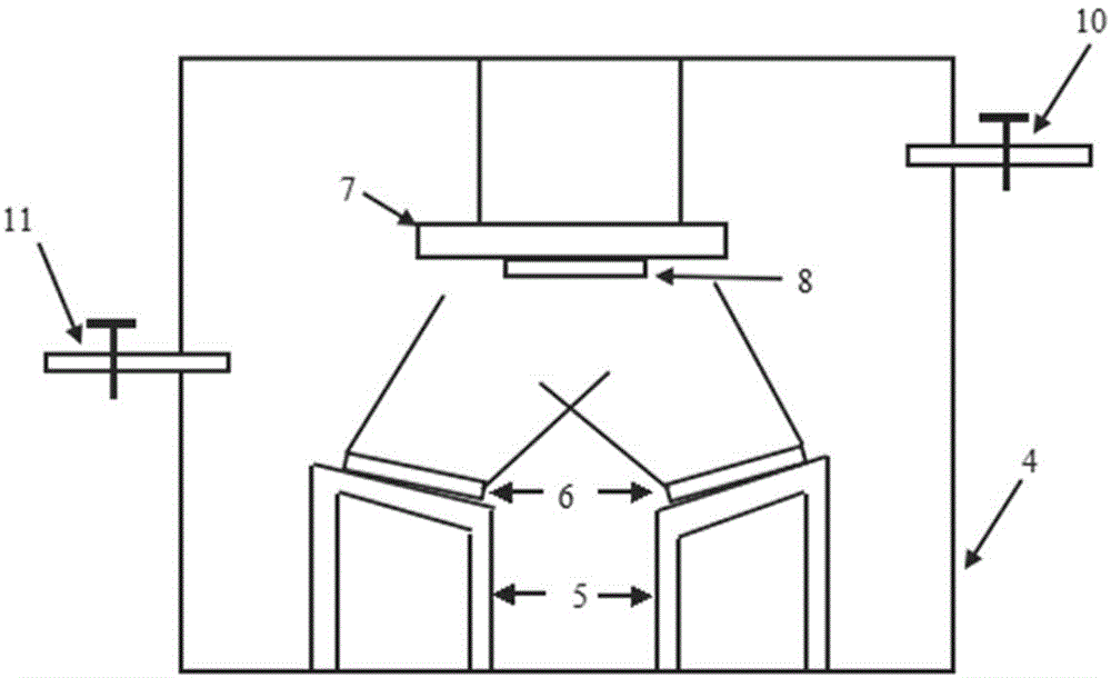
[0040] Such as figure 2 As shown, open the chamber 4 of the magnetron sputtering equipment, take out the tablet press table 8, polish it with sandpaper until it shines, clean the polished waste and organ...


PUM

PropertyMeasurementUnit
Thicknessaaaaaaaaaa
Thicknessaaaaaaaaaa
Diameteraaaaaaaaaa

Abstract

The invention provides a misunderstanding prevention resistance random access memory and a production method thereof. The structure of the resistance random access memory lies in that a resistance random medium layer and an Ag electrode membrane layer are sequentially formed on a Pt membrane layer of a Pt/Ti/SiO2/Si substrate; the resistance random medium layer comprises a first ferrite bismuth membrane layer, a second ferrite bismuth doped silver membrane layer and a third ferrite bismuth membrane layer which are sequentially formed. By the arrangement, stable resistance changes are presented, resistances of high-low resistance states are quite concentrated in distribution, and the high resistance and the low resistance are large in difference, so that confusion of the high and low resistances is less prone to occurrence, and misunderstanding is not easy to occur during data reading. The resistance random access memory is remarkable in switch effect and quite beneficial to readout of the memory. In addition, anti-fatigue performance of the resistance random access memory under the high-low resistance states is quite good.

Description

technical field [0001] The invention relates to a memory, in particular to a resistive memory which can avoid misreading and a preparation method thereof. Background technique [0002] In recent years, nano-scale resistive switching Radom Access Memory (RRAM) has become a popular technology due to its super memory function, ultra-fast switching speed, excellent fatigue resistance, excellent scalability and CMOS compatibility. It is one of the strong candidates for next-generation high-density memory and has been extensively studied. RRAM is a typical two-terminal metal-based metal-dielectric layer-metal sandwich structure. It mainly uses the reversible transition phenomenon between the high and low resistance states of the intermediate dielectric layer under the action of different electric excitations to store data. [0003] At present, researchers have discovered a variety of intermediate dielectric layer materials, including perovskite oxides, binary transition metal ox...

Claims


Application Information

Patent Timeline
IPC IPC(8): H01L45/00C23C14/35C23C14/08C23C14/18C23C14/04
Inventor 闫小兵陈建辉陈英方
Owner HEBEI UNIVERSITY
Why Eureka
Try Eureka