
Method for preparing silicon nanostructured material based on external electric field

A technology of structural materials and external electric field, applied in the direction of nanotechnology, chemical instruments and methods, crystal growth, etc., can solve the problems of complicated operation and difficult control, and achieve the effect of simple and easy method, which is conducive to large-scale production

Active Publication Date: 2015-08-05
王颐疆
View PDF4 Cites 7 Cited by
  • Summary
  • Abstract
  • Description
  • Claims
  • Application Information

AI Technical Summary

Problems solved by technology

At present, most of the methods in the world use methods such as changing the proportion of oxidant and the shape or surface morphology of the catalyst to control the direction of corrosion preparation. However, these methods have defects such as complicated operation and difficult control.

Method used


Image

  • Method for preparing silicon nanostructured material based on external electric field

Examples


Embodiment 1

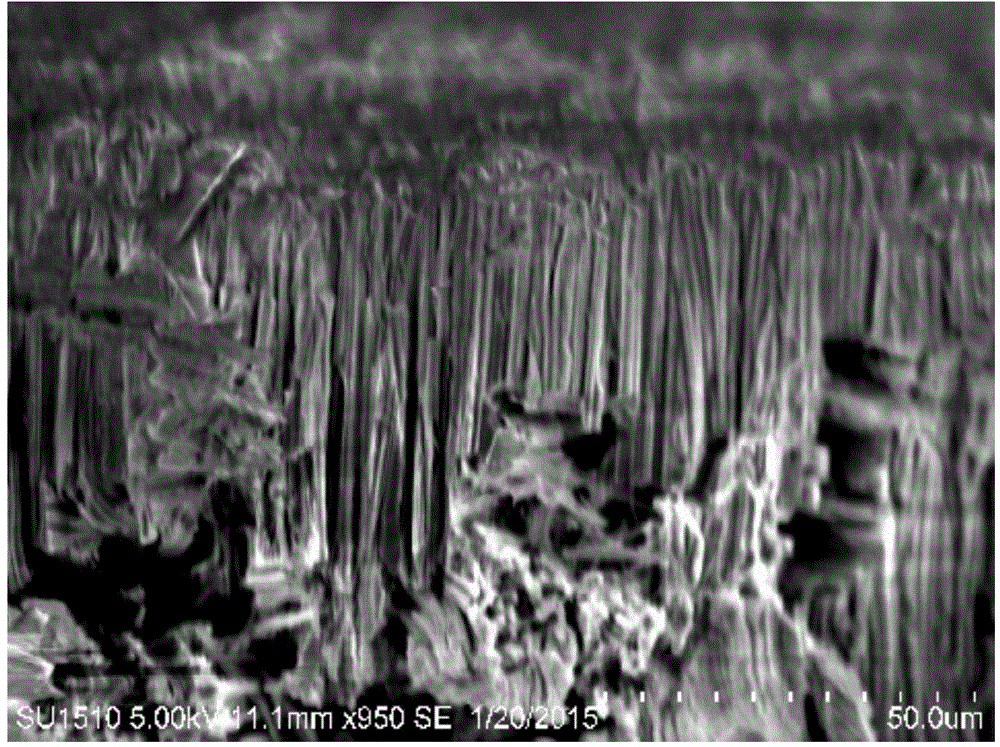
[0019] Put the clean monocrystalline silicon (100) into the mixed solution of silver nitrate and hydrofluoric acid to deposit a layer of silver film on the surface of the silicon wafer, and then quickly put it into the corrosion solution. The corrosion solution is filled in the container, and the two sides of the container are fixed. A pair of graphite electrodes, the graphite electrodes are immersed in the corrosion solution. The proportion of components of the corrosion solution is hydrofluoric acid: hydrogen peroxide at a volume ratio of 12:1, the mass concentration of hydrofluoric acid is 40%, and the mass concentration of hydrogen peroxide is 30%. Turn on the power supply of the graphite electrode, keep the voltage at 1.4mV, corrode at 15°C-25°C for 90min, take it out, wash and dry it, and obtain the silicon nanowire structure.

Embodiment 2

[0021] Put the clean monocrystalline silicon (110) into the mixed solution of silver nitrate and hydrofluoric acid to deposit a layer of silver film on the surface of the silicon wafer, and then quickly put it into the corrosion solution. The corrosion solution is filled in the container, and the two sides of the container are fixed. A pair of graphite electrodes, the graphite electrodes are immersed in the corrosion solution. The proportion of components of the corrosion solution is hydrofluoric acid: hydrogen peroxide at a volume ratio of 12:1, the mass concentration of hydrofluoric acid is 40%, and the mass concentration of hydrogen peroxide is 30%. Turn on the graphite electrode power supply, keep the voltage at 5mV, corrode at 15°C-25°C for 90min, take it out, wash and dry it, and obtain a silicon nanowire structure.

Embodiment 3

[0023] Put the clean monocrystalline silicon (111) into the mixed solution of silver nitrate and hydrofluoric acid to deposit a layer of silver film on the surface of the silicon wafer, and then quickly put it into the corrosion solution. The corrosion solution is filled in the container, and the two sides of the container are fixed. A pair of graphite electrodes, the graphite electrodes are immersed in the corrosion solution. The proportion of components of the corrosion solution is hydrofluoric acid: hydrogen peroxide at a volume ratio of 12:1, the mass concentration of hydrofluoric acid is 40%, and the mass concentration of hydrogen peroxide is 30%. Turn on the power supply of the graphite electrode, keep the voltage at 8mV, corrode at 15°C-25°C for 90min, take it out, wash and dry it, and obtain a silicon nanowire structure.

[0024] The invention belongs to the technical field of preparing silicon nanostructure materials, and in particular relates to a method for preparin...


PUM


Abstract

The invention discloses a method for preparing a silicon nanostructured material based on an external electric field. The method comprises the following steps: (1) putting a clean silicon wafer into a mixed solution of hydrofluoric acid and silver nitrate to deposit a layer of silver film on the surface of the silicon wafer; (2) immediately putting the coated silicon wafer from the step (1) into a corrosive liquid, wherein the corrosive liquid is contained in a container; a pair of noble electrodes are fixed to two sides of the container; and the noble electrodes are immersed in the corrosive liquid; and (3) immediately turning on a power supply of the noble electrodes after the step (2) and corroding for a period of time to obtain the silicon nanostructured material. Only by changing a single variable of electric field, corrosion path of catalyst granules can be controlled according to the method. The method is simple and easy to operate and is beneficial to large-scale production. In addition, applicability of the silicon nanostructured material in aspects of solar cells, lithium ion batteries, thermo-electric devices, precision sensors and the like is enhanced.

Description

technical field [0001] The invention belongs to the technical field of preparing silicon nanostructure materials, and in particular relates to a method for preparing silicon nanostructure materials based on an external electric field. Background technique [0002] Silicon nanostructure materials play a very important role in the fields of sensors, solar cells, MEMS and so on. At present, there are many methods for preparing silicon nanostructure materials at home and abroad, mainly chemical vapor deposition and oxide-assisted growth methods, but these methods require complex conditions and require high equipment. [0003] Metal-assisted chemical etching is also one of the current preparation methods for silicon nanostructure materials. It is widely accepted and used at home and abroad due to its advantages of simple operation, no need for complicated equipment and harsh conditions. However, in the process of preparing silicon nanowire structures by etching, the etchant alwa...

Claims


Application Information

Patent Timeline
IPC IPC(8): C30B33/10C25F3/14C25F3/12B82Y40/00
Inventor 巢炎焦晓东郑武永姚安琦吴立群
Owner 王颐疆
Learn More