n-type ldmos device and process method

A process method, N-type technology, applied in the fields of semiconductor devices, semiconductor/solid-state device manufacturing, electrical components, etc., can solve the problems of unsatisfactory breakdown voltage, high surface electric field strength, no electric field distribution optimization, etc., to improve the potential distribution. , the effect of reducing the electric field strength and increasing the breakdown voltage

Active Publication Date: 2018-08-21
SHANGHAI HUAHONG GRACE SEMICON MFG CORP
View PDF5 Cites 0 Cited by
  • Summary
  • Abstract
  • Description
  • Claims
  • Application Information

AI Technical Summary

Problems solved by technology

This structure does not optimize the electric field distribution of the device, the electric field intensity on the surface is high, and the breakdown voltage is not ideal

Method used


Image

  • n-type ldmos device and process method
  • n-type ldmos device and process method
  • n-type ldmos device and process method

Examples


Embodiment Construction

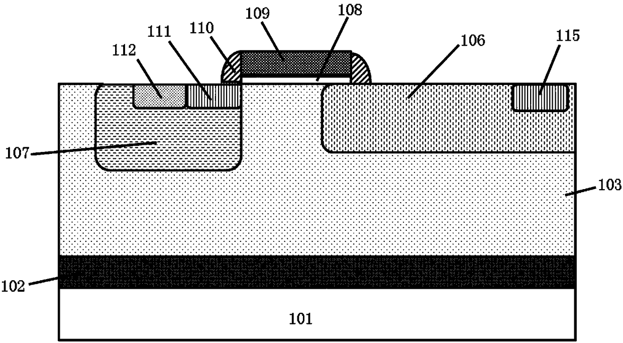
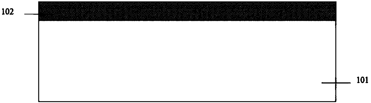
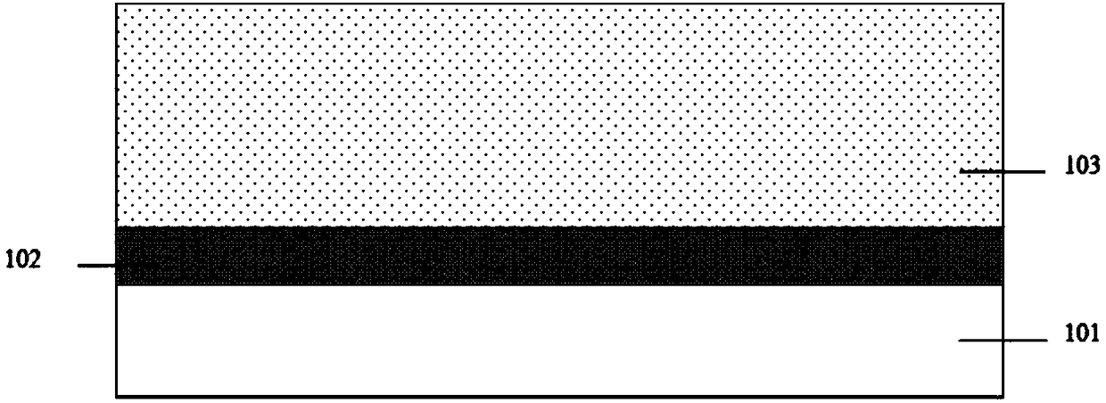
[0023] The N-type LDMOS device described in the present invention, such as Figure 7 As shown, there is an N-type buried layer 102 on the P-type substrate 101, and an N-type deep well 103 is on the buried layer 102; a P well 107 is provided in the N-type deep well 103, and the P well 107 contains heavily doped The P-type region 112 and the source region 111 of the LDMOS device, the silicon substrate surface has a gate oxide layer 108 and a polysilicon gate 109; the N-type deep well 103 also has a drain region 115 of the LDMOS device, and the lead 114 passes through the contact The hole 113 leads out the heavily doped P-type region 112, the source region 111 and the drain region 115; the heavily doped P-type region 112 and the source region 111 in the P well 107 are isolated by the STI field oxygen 104, and the LDMOS device In the drift region, there are STI field oxygen 104 on both sides of the drain region 115, and the drift region is a layered drift region with different dep...


PUM


Abstract

The invention discloses an N-type LDMOS device. An N type buried layer is arranged on a P-type substrate, and an N-type deep well is on the N-type buried layer. A P well is in the N-type deep well and comprises a heavily doped P-type region and the source region of the LDMOS device. The surface of the silicon substrate is provided with a gate oxide layer and a polysilicon gate. The N-type deep well also comprises the drain region of the LDMOS device, and the heavily doped P-type region, the source region and the drain region are led out through contact holes. The heavily doped P-type region and the source region in the P well are isolated by an STI field oxide. Two sides of the drain region in the drift region of the LDMOS device are provided with the STI field oxide. The drift region is a hierarchical drift region with different depths formed by injecting different energies. The invention also discloses the process method of the N-type LDMOS device, and the method can be integrated in a BCD process.

Description

technical field [0001] The invention relates to the field of semiconductors, in particular to an N-type LDMOS device, and also relates to a process method for the N-type LDMOS device. Background technique [0002] DMOS is currently widely used in power management circuits due to its high voltage resistance, high current drive capability and extremely low power consumption. In the BCD process, although DMOS and CMOS are integrated in the same chip, due to the requirements of high withstand voltage and low on-resistance, the conditions of DMOS in the background area and drift area are shared with the existing process conditions of CMOS. , there is a contradiction between the on-resistance and the breakdown voltage, which often cannot meet the requirements of the switch tube application. In LDMOS devices, on-resistance is an important indicator. Therefore, in order to make high-performance LDMOS, it is necessary to adopt various methods to optimize the on-resistance and break...

Claims


Application Information

Patent Timeline
Patent Type & Authority Patents(China)
IPC IPC(8): H01L29/78H01L29/06H01L21/762H01L21/336
CPCH01L29/7816H01L29/0653H01L29/0878H01L29/66689
Inventor 石晶钱文生
Owner SHANGHAI HUAHONG GRACE SEMICON MFG CORP
Why Eureka
Try Eureka