

Electromagnetic shielding optical window making method
An electromagnetic shielding and manufacturing method technology, applied in the field of optical windows, can solve the problems of reducing the light transmission performance and electromagnetic shielding performance of the optical window, uneven distribution of high-order diffraction energy, reducing the light transmission performance of the optical window, etc., so as to achieve good electromagnetic shielding. performance, good light transmission performance, the effect of improving light transmission performance
- Summary
- Abstract
- Description
- Claims
- Application Information
AI Technical Summary
Problems solved by technology
Method used
Image

Examples
specific Embodiment 1
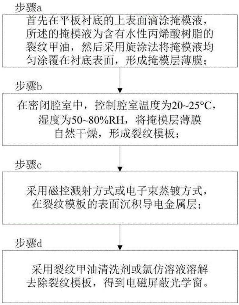
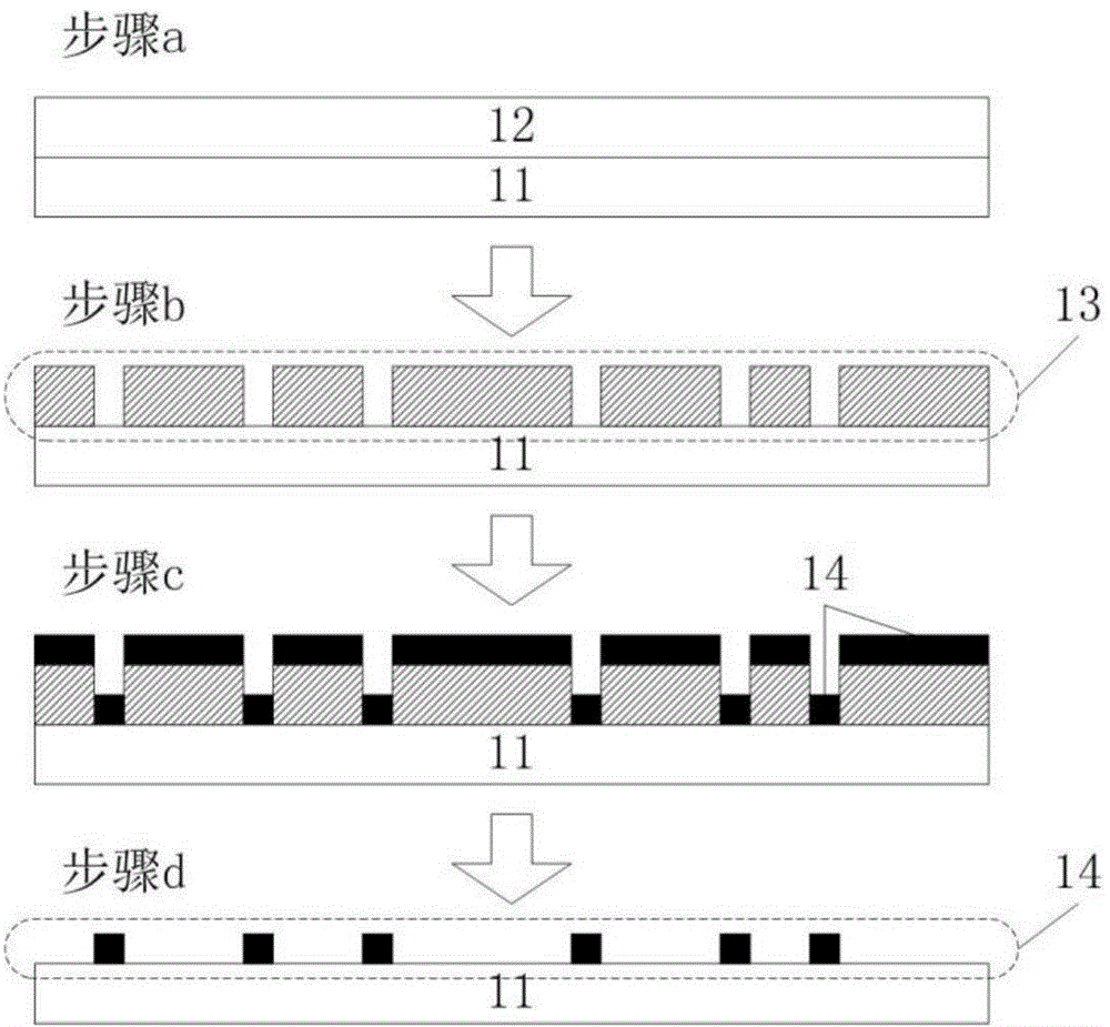
[0039] The manufacturing method of the electromagnetic shielding optical window of the present embodiment, the flowchart is as follows figure 1 As shown, the method includes the following steps:
[0040] In step a, first drop-coat a masking liquid on the upper surface of the flat substrate 11, the masking liquid is cracked nail polish containing water-based acrylic resin, and then uniformly coat the masking liquid on the surface of the substrate by a spin coating method , forming a mask layer film 12;
[0041] Step b, in a closed chamber, control the temperature of the chamber to 20-25°C and the humidity to 50-80% RH, and dry the mask layer film 12 naturally to form the crack template 13;
[0042] Step c, using magnetron sputtering or electron beam evaporation to deposit a conductive metal layer 14 on the surface of the cracked template 13;
[0043] In step d, the cracked template 13 is dissolved and removed with a cracked nail polish cleaning agent or a chloroform solution ...
specific Embodiment 2
[0046] The manufacturing method of the electromagnetic shielding optical window of this embodiment, the method flow and process flow are exactly the same as the specific embodiment 1, the difference is that the limited cracked nail polish is diluted with a diluent, and the dilution ratio k is defined as the volume of the diluent and the cracked nail polish ratio, and 1≤k≤7.
[0047] Under the above-mentioned ratio conditions, it is found that the relationship between the average crack width w of the crack template 13 and the thickness h of the mask layer film 12 is:
[0048] w=0.342e 0.266h
[0049] In the formula, w is the average crack width of the crack template 13 in μm; h is the thickness of the mask layer film 12 in μm.
[0050] The relationship between the average crack interval d of the crack template 13 and the thickness h of the mask layer film 12 is:
[0051] d=15.8e 0.169h
[0052] In the formula, d is the average crack interval of the crack template 13 in μm;...
PUM
| Property | Measurement | Unit |
|---|---|---|
| Thickness | aaaaa | aaaaa |
| Thickness | aaaaa | aaaaa |
| Thickness | aaaaa | aaaaa |
Abstract
Description
Claims
Application Information