Transparent conductive oxide film based on TiN interlayer doping

An oxide film, transparent conductive technology, applied in the direction of the conductive layer on the insulating carrier, can solve the problems of low conductivity, low light loss, low conductivity, etc., to increase the light absorption area, good conductivity, and improve device performance. Effect

Active Publication Date: 2015-08-12
ZHEJIANG UNIV
View PDF4 Cites 2 Cited by
  • Summary
  • Abstract
  • Description
  • Claims
  • Application Information

AI Technical Summary

Problems solved by technology

Solar cells require the front electrode to have high transmittance, high conductivity and extremely low light loss, while the conductivity of traditional TCO films is still low compared to other electrode materials, and in general, the film transmittance and Conductivity is contradictory

Method used


Image

  • Transparent conductive oxide film based on TiN interlayer doping

Examples


Embodiment 1

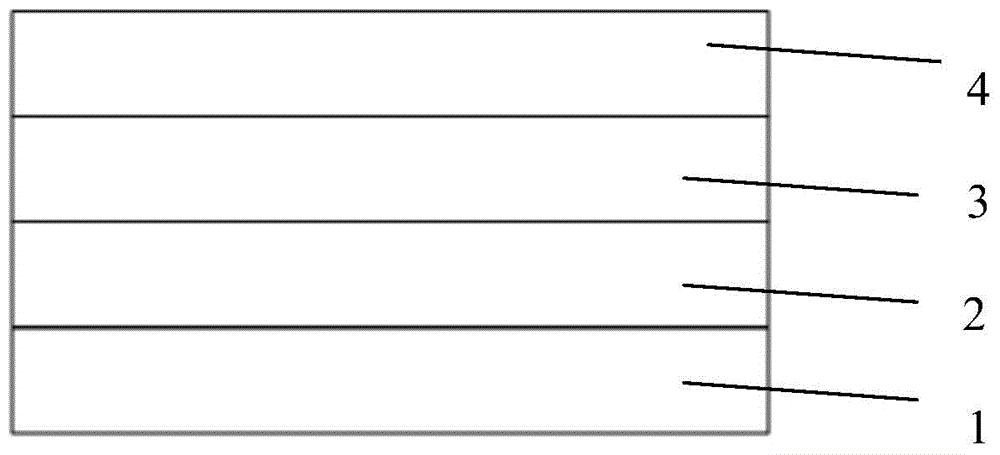
[0022] A transparent conductive oxide film based on TiN interlayer doping, including a substrate 1 (the substrate in this embodiment is a glass substrate), on which a lower transparent conductive layer 2 and an interlayer 3 are grown sequentially from bottom to top And the upper transparent conductive layer 4, the lower transparent conductive layer 2 and the upper transparent conductive layer 4 are transparent conductive oxide layers, wherein the thickness of the lower transparent conductive layer 2 and the upper transparent conductive layer 4 are both ITO films, and the thickness is 30nm. In this implementation, the interlayer 3 is a TiN layer with a thickness of 8 nm.

[0023] The transparent conductive oxide film based on TiN interlayer doping in this embodiment is prepared by the following steps:

[0024] (1) A layer of ITO film is grown by magnetron sputtering on the glass substrate after cleaning (sequentially cleaned by acetone, ethanol, and deionized water for 10 minut...


PUM

PropertyMeasurementUnit
thicknessaaaaaaaaaa
thicknessaaaaaaaaaa
thicknessaaaaaaaaaa

Abstract

The present invention discloses a transparent conductive oxide film based on TiN interlayer doping, comprising a substrate, wherein a lower transparent conducting layer, an interlayer and an upper transparent conducting layer successively grow on the substrate from the bottom up, the lower transparent conducting layer and the upper transparent conducting layer are transparent conductive oxide layers, and the interlayer is a TiN layer. According to the transparent conductive oxide film of the present invention, a TiN film (i.e., the interlayer) is doped in a traditional TCO film, in this way, carrier concentration of the film is increased, carrier mobility is raised, and optical performance of the film of changed, so that the film can be matched with medium within a near-infrared band to generate plasma resonance, therefore, the transparent conductive oxide film can be applied to the field of optical devices within the near-infrared band, in addition, TiN is rich in source and low in price, thereby facilitating commercial promotion and application.

Description

technical field [0001] The invention relates to the technical field of photoelectric materials, in particular to a transparent conductive oxide film based on TiN interlayer doping. Background technique [0002] With the development of social science, the demand for functional materials is increasingly urgent. New functional materials have become the key to the development of new technologies and industries. In recent years, surface plasmon technology has received more and more attention. Noble metal materials such as gold and silver have been widely used in optoelectronic material devices such as surface plasmons because of their low ohmic loss and high electrical conductivity. [0003] However, precious metal materials such as gold and silver still have certain limitations. Compared with electrical properties, their optical properties are poor, especially in the near-infrared band (wavelength range between 1 μm and 3 μm), and the optical loss is very high. , the optical p...

Claims


Application Information

Patent Timeline
Patent Type & Authority Applications(China)
IPC IPC(8): H01B5/14
Inventor 叶辉张诗雨方旭
Owner ZHEJIANG UNIV
Why Eureka
Try Eureka