A method for fabricating a T-gate of a high ion mobility transistor

A technology of ion mobility and fabrication method, applied in the field of T-type gate fabrication, can solve the problems of large line width, high fabrication cost and low production efficiency in photoresist open area, and achieve fast exposure speed, low cost and production efficiency high effect

Active Publication Date: 2018-05-01
XIAMEN SANAN INTEGRATED CIRCUIT
View PDF4 Cites 0 Cited by
  • Summary
  • Abstract
  • Description
  • Claims
  • Application Information

AI Technical Summary

Problems solved by technology

The investment of E-beam equipment is high, and because the exposure is performed by scanning, the production efficiency is extremely low, and the production capacity is too small, which leads to high manufacturing costs and is difficult to promote and apply in actual production
However, the line width of the photoresist opening area formed by other known photolithography equipment is relatively large, and it is difficult to directly form a window below 0.13 μm for making T-shaped grids, which limits its production in small-sized T-shaped grids. application in

Method used


Image

  • A method for fabricating a T-gate of a high ion mobility transistor

Examples


Embodiment Construction

[0027] The present invention will be described in further detail below in conjunction with the accompanying drawings and embodiments. The drawings of the present invention are only schematic diagrams for easier understanding of the present invention, and their specific proportions can be adjusted according to design requirements. Those skilled in the art should understand that the upper and lower relationships of relative components in the figures described herein refer to the relative positions of the components, so all of them can be turned over to present the same components, which should all fall within the scope of the present specification.

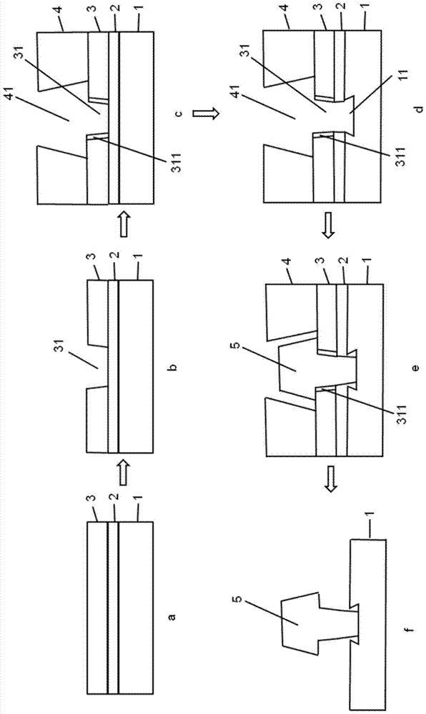
[0028] refer to figure 1 Middle a-f is the flow chart of the manufacturing method of the present invention. Such as figure 1 As shown in a, a GaAs-based substrate 1 is provided, an anti-reflection layer 2 is formed on the substrate, and a first photoresist 3 is coated on the anti-emission layer 2 . Specifically, the anti-reflecti...


PUM


Abstract

The invention discloses a fabrication method of the T type gate of a high-ion mobility transistor. The method includes the following steps that: an anti-reflection layer and first photoresist are sequentially formed on a gallium arsenide (GaAs) substrate; the first photoresist is subjected to exposure and development, so that a display area of which the width ranges from 0.16 to 0.19 microns can be formed, and the display area is further subjected to a chemical shrinkage process, so that the width of the display area can be decreased to a range from 0.11 to 0.13 microns; and the display area of the first photoresist is coated with second photoresist, and the second photoresist is subjected to exposure and development, so that the exposed and developed second photoresist and the display area of the first photoresist can jointly form an etching window of the T type gate, and the T type gate of which the width ranges from 0.11 to 0.13 microns can be formed through metal deposition. The fabrication method of the invention has the advantages of low equipment input and high production capacity, and can effectively reduce production cost and is suitable for practical production application.

Description

technical field [0001] The invention relates to a semiconductor process, in particular to a method for manufacturing a T-shaped gate of a high ion mobility transistor. Background technique [0002] A high ion mobility transistor (HEMT) utilizes the two-dimensional electron gas layer (2-DGE) existing at the heterojunction interface, and controls the electron concentration of the 2-DGE between the source and the drain by changing the gate pressure, thereby Control work status. HEMTs are a new generation of transistors that are the first choice for high-frequency, high-voltage, high-temperature and high-power applications due to their excellent performance. [0003] The fabrication of the gate of the HEMT has a crucial influence on the cut-off frequency of the device. Generally speaking, the smaller the gate length and the lower the gate resistance, the higher the cutoff frequency of the device. In order to take into account the small gate length and low gate resistance, the...

Claims


Application Information

Patent Timeline
Patent Type & Authority Patents(China)
IPC IPC(8): H01L21/28H01L21/027
CPCH01L21/0274H01L21/28
Inventor 郭佳衢罗怡弦
Owner XIAMEN SANAN INTEGRATED CIRCUIT
Why Eureka
Try Eureka