Compound semiconductor device and manufacturing method thereof
A compound semiconductor and manufacturing method technology, applied in semiconductor/solid-state device manufacturing, semiconductor devices, electric solid-state devices, etc., can solve problems such as increasing costs, achieve the effects of increasing difficulty, alleviating charge sensitivity, and optimizing surface field distribution
- Summary
- Abstract
- Description
- Claims
- Application Information
AI Technical Summary
Problems solved by technology
Method used
Image

Examples
no. 1 example
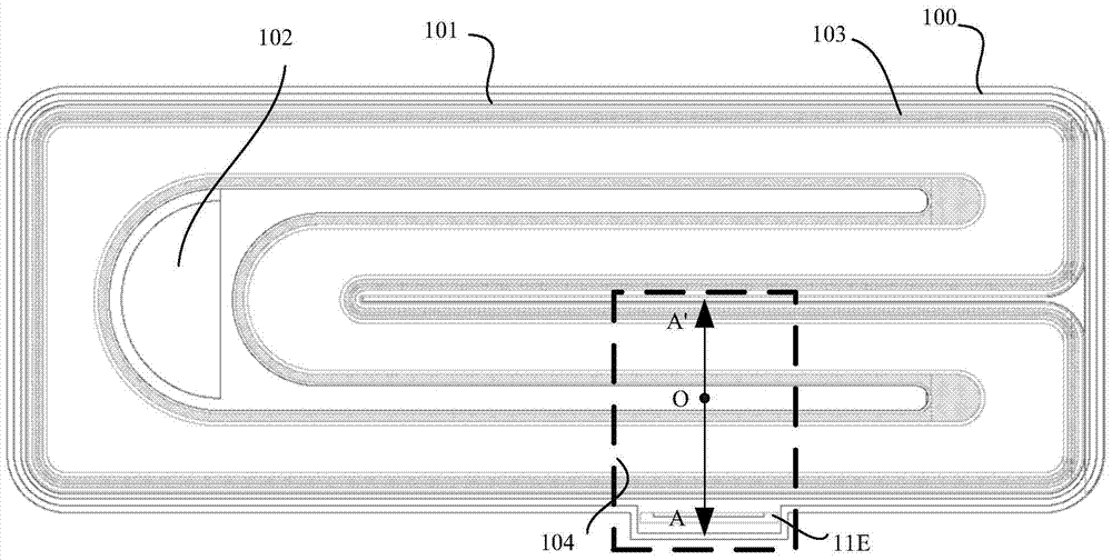
[0076] refer to figure 1 , figure 1 A complete layout of the compound semiconductor device according to the present embodiment is shown. The device layout in this embodiment is an interdigitated layout to obtain sufficient current capability. Such as figure 1 As shown, the layout mainly includes a drain portion 102 , a source portion 101 , a gate portion 103 , and a ground portion 100 . The straight-side area 104 framed by the dotted line is part of the actual conductive area, and other parts are connected in parallel with it. A transistor (for example, an LDMOS transistor in this embodiment) and a squeeze resistor are integrated in the compound semiconductor device, and the transistor and the squeeze resistor have a common drain to form a common drain structure. The common drain structure can make the product layout more compact, thereby saving chip area.
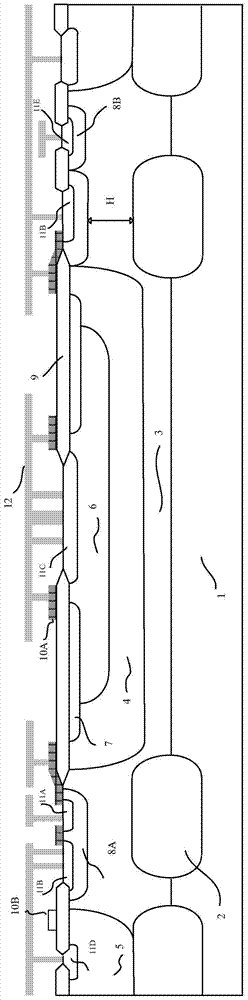
[0077] refer to figure 2 , figure 2 show figure 1 Schematic diagram of the cross-sectional mechanism of the mi...
no. 2 example
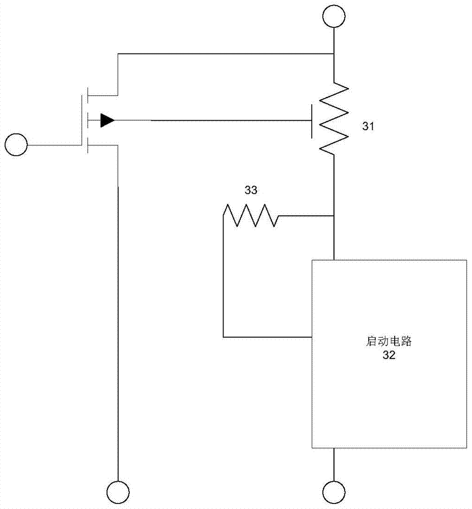
[0084] Such as image 3 As shown, in practical applications, such as power supply or AC-LED applications, the startup circuit 32 is usually required. When the circuit is started, the squeeze resistor 31 needs to be turned on and the starting circuit 32 is charged, and the circuit works normally after the charging is completed. At this time, the source of the squeeze resistor 31 is raised above 10V, and the squeeze resistor 31 is turned off. At this time, only a small current (for example, below 10 μA) flows from image 3 The resistance 33 on the left side flows through, then according to R=V / I estimation, this resistance 33 needs at least 1M ohm. At present, there are many 2K resistors used in the general process, and in order to ensure the accuracy of the resistor, the general resistor width is more than 2μm, so the 1M ohm resistor requires a very large length of the resistor (for example, more than 2000μm).
[0085] If such a large resistance is separately arranged outside...
no. 3 example
[0087] refer to Figure 5 , Figure 5 Another compound semiconductor device provided according to the third embodiment is shown. Figure 5 corresponds to figure 1 The straight-edge region 104 in the figure 1 The straight edge region 104 of is cut along AA' to get Figure 5 The sectional view shown. The third embodiment and figure 2 The device structure of the first embodiment shown is basically the same, the difference is that the doping types of all layers in the device structure are opposite to those of the first embodiment, thereby forming a P-type LDMOS transistor.
PUM
 Abstract
Description
Claims
Application Information
 - R&D
- Intellectual Property
- Life Sciences
- Materials
- Tech Scout
- Unparalleled Data Quality
- Higher Quality Content
- 60% Fewer Hallucinations
Browse by: Latest US Patents, China's latest patents, Technical Efficacy Thesaurus, Application Domain, Technology Topic, Popular Technical Reports.
© 2025 PatSnap. All rights reserved.Legal|Privacy policy|Modern Slavery Act Transparency Statement|Sitemap|About US| Contact US: help@patsnap.com