Copper alloy for electrical and electronic equipment, copper alloy thin sheet for electrical and electronic equipment, and conductive part and terminal for electrical and electronic equipment

A technology for electronic and electrical and conductive components is applied in the fields of copper alloys for electronic and electrical equipment, copper alloy sheets for electronic and electrical equipment, conductive components and terminals for electronic and electrical equipment, and can solve the problems of improving stress relaxation resistance, rising material costs, and no Considering the stress relaxation resistance of the P compound, it achieves the effect of excellent bending workability and excellent bending balance

Active Publication Date: 2015-09-09
MITSUBISHI MATERIALS CORP +1
View PDF10 Cites 3 Cited by
  • Summary
  • Abstract
  • Description
  • Claims
  • Application Information

AI Technical Summary

Problems solved by technology

[0016] However, in Patent Documents 1 and 2, only the respective contents of Ni, Fe, and P are considered, and it is not always possible to reliably and sufficiently improve the stress relaxation resistance simply by adjusting these respective contents.
[0017] In addition, although Patent Document 3 discloses adjusting the Ni/Sn ratio, the relationship between the P compound and the stress relaxation resistance is not considered at all, and the improvement of the stress relaxation resistance cannot be sufficiently and reliably achieved.
[0018] Furthermore, in Patent Document 4, the stress relaxation resistance cannot be sufficiently improved only by adjusting the t

Method used


Image

  • Copper alloy for electrical and electronic equipment, copper alloy thin sheet for electrical and electronic equipment, and conductive part and terminal for electrical and electronic equipment
  • Copper alloy for electrical and electronic equipment, copper alloy thin sheet for electrical and electronic equipment, and conductive part and terminal for electrical and electronic equipment
  • Copper alloy for electrical and electronic equipment, copper alloy thin sheet for electrical and electronic equipment, and conductive part and terminal for electrical and electronic equipment

Examples


Embodiment

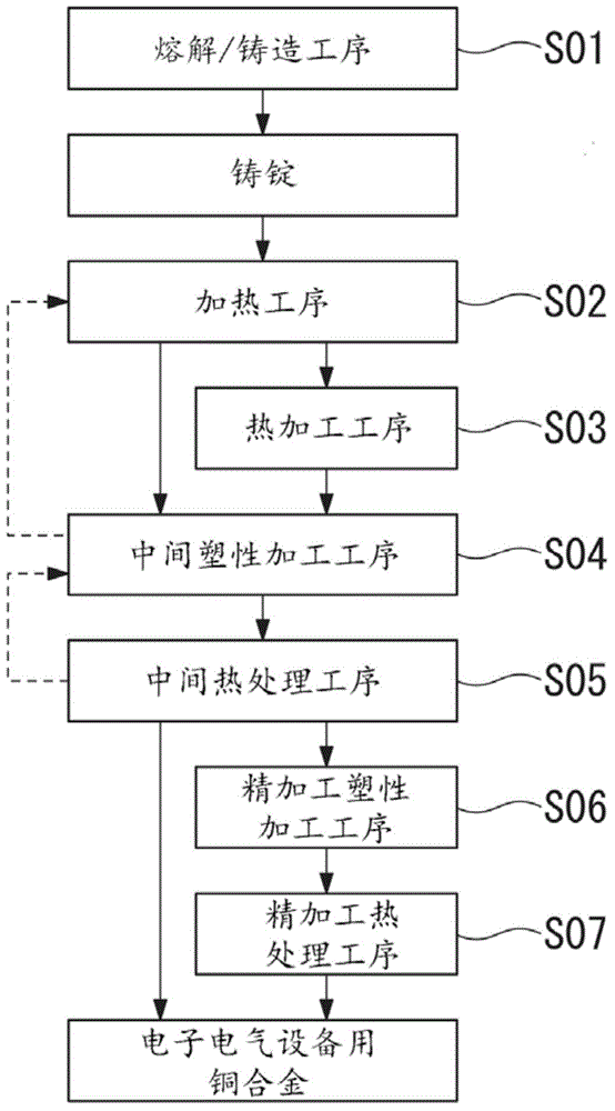
[0139]Hereinafter, the results of confirmation experiments conducted to confirm the effects of the present invention are shown together with comparative examples as examples of the present invention. In addition, the following examples are examples for illustrating the effects of the present invention, and the structures, processes and conditions described in the examples do not limit the technical scope of the present invention.

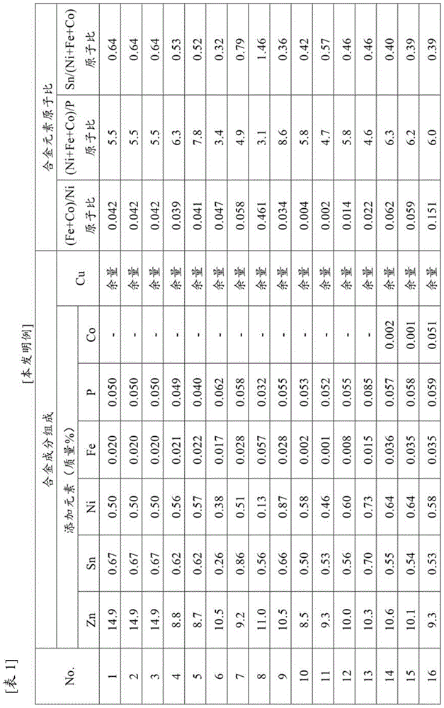
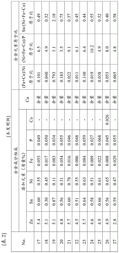
[0140] Raw materials consisting of Cu-40% Zn master alloy and oxygen-free copper (ASTM B152 C10100) with a purity of 99.99% by mass or more were prepared, and were charged into a high-purity graphite crucible, and placed in a N 2 Melting was performed using an electric furnace under a gas atmosphere. Various additive elements were added to copper alloy molten metal, alloy molten metal having the composition shown in Tables 1, 2, 3, and 4 was melted, and poured into a carbon mold to produce an ingot. In addition, the size of the ingot was about 40 m...


PUM


Abstract

The present invention pertains to a copper alloy for electrical and electronic equipment, a copper alloy thin sheet for electrical and electronic equipment, and a conductive part and terminal for electrical and electronic equipment. The copper alloy for electrical and electronic equipment contains more than 2.0 mass% to 15.0 mass% of zinc, 0.10 mass% to 0.90 mass% of tin, 0.05 mass% to less than 1.00 mass% of nickel, 0.001 mass% to less than 0.100 mass% of iron, and 0.005 mass% to 0.100 mass% of phosphorus, with the remainder comprising copper and unavoidable impurities. The copper alloy satisfies 0.002 ≤ Fe/Ni < 1.500, 3.0 < (Ni + Fe)/P < 100.0, and 0.10 < Sn/(Ni + Fe) < 5.00 in terms of atomic ratios. The yield ratio (YS/TS), which is calculated from the tensile strength (TS) and 0.2% offset yield strength (YS) when a tension test is performed in a direction parallel to the rolling direction, is over 90%.

Description

technical field [0001] The present invention relates to a Cu-Zn-Sn based copper alloy for electrical and electronic equipment used as a conductive element for electrical and electronic equipment such as a connector of a semiconductor device, other terminals, or a movable conductive sheet or a lead frame of an electromagnetic relay. Copper alloy sheet for electrical and electronic equipment, conductive components and terminals for electrical and electronic equipment. [0002] This application claims priority to Patent Application No. 2012-288051 filed in Japan on December 28, 2012 and Patent Application No. 2013-252331 filed in Japan on December 5, 2013, and uses the contents thereof for this specification. Background technique [0003] Cu—Zn alloys have been widely used as raw materials for conductive elements for electrical and electronic equipment in view of the balance between strength, processability, and cost. [0004] In addition, in the case of terminals such as conn...

Claims


Application Information

Patent Timeline
IPC IPC(8): C22C9/04H01B1/02H01B5/02C22F1/00C22F1/08
CPCC22F1/08H01B1/026C22C9/04B32B15/01C22C9/00C22C9/06Y10T428/12Y10T428/12431Y10T428/12438Y10T428/12715Y10T428/12882Y10T428/12903Y10T428/1291Y10T428/12917Y10T428/12924B32B15/04B32B15/043B32B15/20C23C2/08C23C30/00C23C30/005H01B5/02
Inventor 牧一诚森广行山下大树
Owner MITSUBISHI MATERIALS CORP
Why Eureka
Try Eureka