

Target material binding method
A target material and non-magnetic metal technology, which is applied in metal material coating process, ion implantation plating, coating, etc., can solve the problems of non-reusable, solder waste, high cost of target material, etc., to increase electrical and thermal conductivity, Effects of reducing cost and controlling the thickness of welding layer
- Summary
- Abstract
- Description
- Claims
- Application Information
AI Technical Summary
Problems solved by technology
Method used
Image

Examples
Embodiment 1
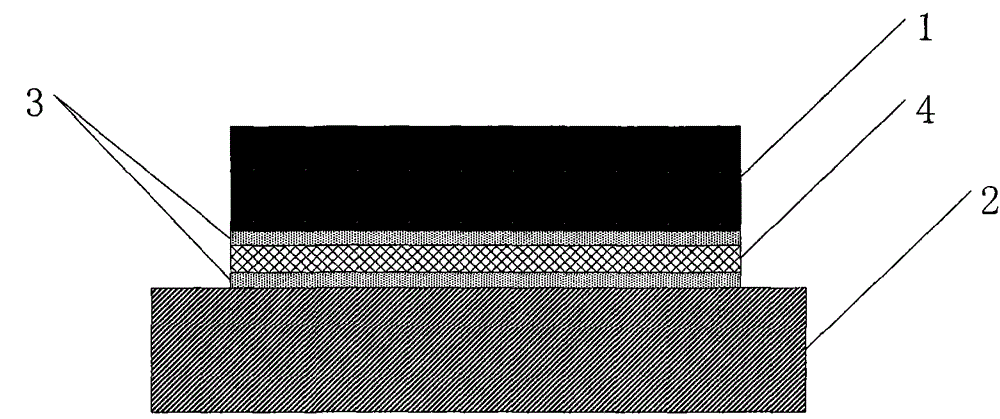
[0031] Follow the steps below to complete the figure 1 Binding of targets of the structures shown:
[0032] (1) Clean the welding surfaces of the target 1 and the back plate 2 with absolute ethanol;
[0033] (2) adding 60% by weight aluminum powder to the epoxy resin glue to make conductive glue 3, wherein the particle size of the aluminum powder is 1-120 μm;
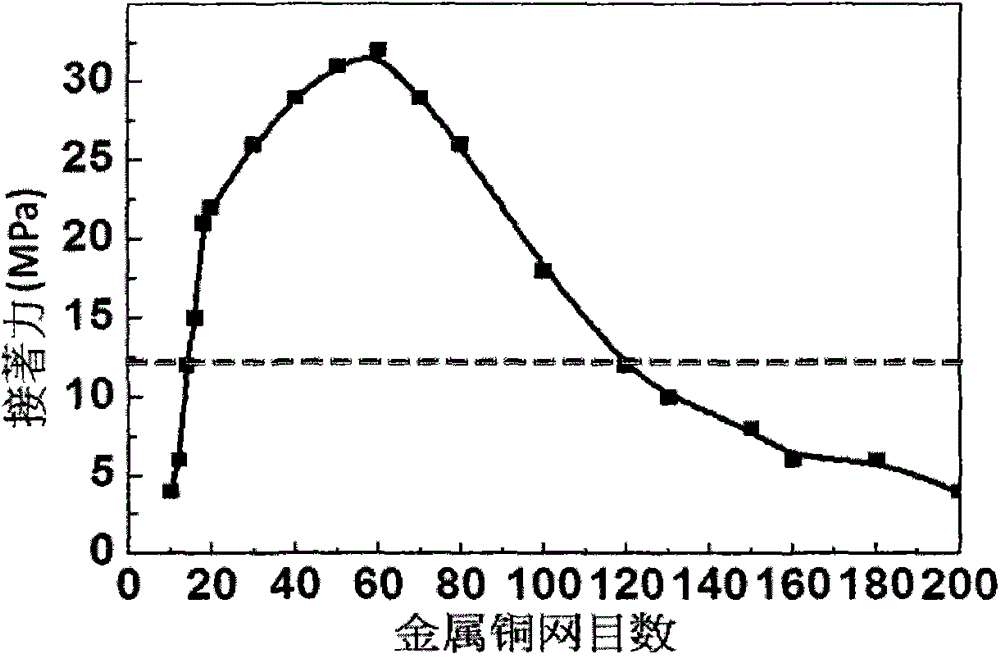
[0034] (3) The conductive adhesive 3 is evenly coated on the welding surface of the target 1 and the back plate 2 and both sides of the copper mesh 4, wherein the mesh size of the copper mesh 4 is 20 mesh, and the copper mesh 4 The wire diameter of the net 4 is 0.15mm;
[0035] (4) The copper mesh 4 and the target material 1 are sequentially stacked on the welding surface of the back plate 2 and positioned, and the copper mesh 4 is located between the welding surface of the target material 1 and the back plate 2;
[0036] (5) Place a briquette on the target 1, and stand and solidify at normal temperature and pressure...
Embodiment 2
[0040] Follow the steps below to complete the figure 1 Binding of targets of the structures shown:
[0041] (1) Clean the welding surfaces of the target 1 and the back plate 2 with isopropanol;
[0042] (2) adding 60% by weight aluminum powder to the epoxy resin glue to make conductive glue 3, wherein the particle size of the aluminum powder is 1-120 μm;
[0043] (3) The conductive adhesive 3 is evenly coated on the welding surface of the target 1 and the back plate 2 and both sides of the copper mesh 4, wherein the mesh size of the copper mesh 4 is 22 mesh, and the copper mesh 4 The wire diameter of the net 4 is 0.15mm;
[0044] (4) The copper mesh 4 and the target material 1 are sequentially stacked on the welding surface of the back plate 2 and positioned, and the copper mesh 4 is located between the welding surface of the target material 1 and the back plate 2;
[0045] (5) Place a briquette on the target 1, and stand and solidify at normal temperature and pressure to o...
Embodiment 3
[0048] It differs from Example 1 in that: the mesh size of the copper mesh 4 is 24 mesh.
PUM
| Property | Measurement | Unit |
|---|---|---|
| Particle size | aaaaa | aaaaa |
Abstract
Description
Claims
Application Information