Forming method of semiconductor structure

A semiconductor and gate structure technology, applied in the field of semiconductor structure formation, can solve problems such as complex process steps, affecting memory reliability, and deterioration of dielectric layer isolation performance, and achieve smooth inner walls, improved inner wall contours, and increased top width Effect

Inactive Publication Date: 2015-09-30
SEMICON MFG INT (SHANGHAI) CORP
View PDF5 Cites 6 Cited by
  • Summary
  • Abstract
  • Description
  • Claims
  • Application Information

AI Technical Summary

Problems solved by technology

[0004] The smaller the distance between adjacent storage units, the difficulty of filling the dielectric material between adjacent storage units will be increased, and it is easy to form voids in the dielectric layer between the adjacent storage units, resulting in the isolation of the dielectric layer. The performance deteriorates, causing problems such as bridging between the bit lines of adjacent memory cells, and it will also increase the difficulty of forming the side walls of the memory cells, thereby affecting the reliability of the memory
[0005] Moreover, on the peripheral chip of the memory unit, peripheral circuit devices, such as input / output transistors, etc. need to be formed. Usually, it is necessary to form sidewalls and filling dielectric layers of the memory cell and peripheral circuit devices respectively, and the process steps are relatively complicated.

Method used


Image

  • Forming method of semiconductor structure
  • Forming method of semiconductor structure
  • Forming method of semiconductor structure

Examples


Embodiment Construction

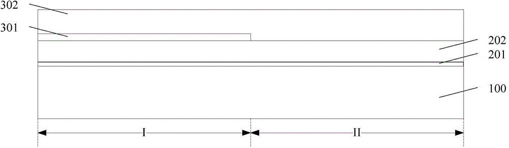
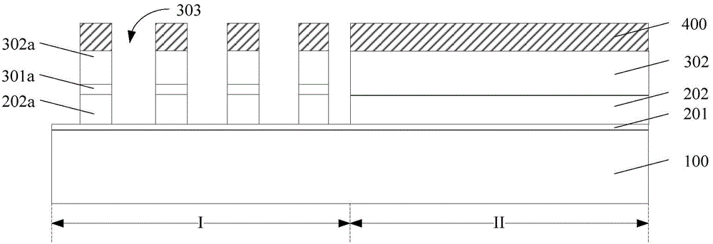
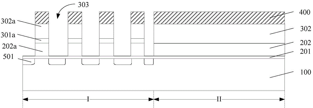
[0029] As mentioned in the background art, due to the small distance between adjacent storage units, it is difficult to fill the space with dielectric materials, and defects such as voids are easily formed, which affects the reliability of the memory.

[0030] In the process of forming the sidewall of the transistor of the peripheral circuit, a chemical vapor deposition process is used. After the sidewall material layer is formed on the semiconductor substrate, the sidewall material layer is etched without a mask to form the side wall. But because the space between the storage units is small, in the process of forming the sidewall material layer, the sidewall material layer will fill up the grooves between the storage units, but due to the space between the storage units Smaller, resulting in a higher aspect ratio of the groove, resulting in more defects such as voids in the side wall material layer filled in the groove. Subsequently, after forming the side walls of the trans...


PUM


Abstract

A forming method of a semiconductor structure includes providing a semiconductor substrate including a first zone having a plurality of separated storage grid structures and a second zone having a plurality of gate structures. First grooves are arranged between adjacent storage grid structures and second grooves are arranged between adjacent gate structures. The width of each first groove is smaller than that of the second groove. A liner layer is formed on the semiconductor substrate. The method also includes etching the liner layer for making the width of the top part of each first groove greater than that of the bottom part of each first groove; forming a second wall material layer on the liner layer; etching the second side wall material layer, forming a second side wall on the surface of the side wall of the gate structures and forming a medium layer filling the first grooves at the same time. By adopting the above method, the semiconductor structure forming technology can be simplified.

Description

technical field [0001] The invention relates to the technical field of semiconductors, in particular to a method for forming a semiconductor structure. Background technique [0002] In the current semiconductor industry, integrated circuit products can be mainly divided into three types: logic, memory and analog circuits, among which memory devices account for a considerable proportion of integrated circuit products. Among them, non-volatile memory is widely used, including: read-only memory, programmable read-only memory, erasable programmable read-only memory, electrically erasable programmable read-only memory, flash memory and ferroelectric memory, etc. [0003] With the continuous improvement of the integration level of semiconductor devices, the size of memory cells in the memory and the distance between adjacent memory cells are also continuously reduced, and the reliability of the memory faces new challenges. [0004] The smaller the distance between adjacent storag...

Claims


Application Information

Patent Timeline
Patent Type & Authority Applications(China)
IPC IPC(8): H01L21/8247H01L21/28
Inventor 陈超杨芸李绍彬
Owner SEMICON MFG INT (SHANGHAI) CORP
Why Eureka
Try Eureka