

Solar cell production process
A technology of solar cells and production processes, applied in circuits, photovoltaic power generation, electrical components, etc., can solve problems such as low degree, edge leakage, damage to PN junction, etc.
- Summary
- Abstract
- Description
- Claims
- Application Information
AI Technical Summary
Problems solved by technology
Method used
Image

Examples
Embodiment 1
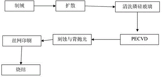
[0020] A solar cell production process, comprising the steps of:
[0021] (1) Texturing, with HF concentration of 5%, HNO 3 The concentration is 40%, the weight loss of the silicon wafer after texturing is about 0.3g, and the size of the textured surface is 3μm;
[0022] (2) Diffusion, heat up the textured silicon wafer to 865°C and pass it through 760 SCCM phosphorus source, 6 SLM nitrogen atmosphere, and 360 SCCM oxygen atmosphere to achieve the purpose of diffusion, and the diffusion resistance is controlled to 75Ω / □ ;
[0023] (3) To clean the phosphorous silicon wafers, clean the phosphorous silicon wafers by means of roller transmission in HF with a concentration of 10%, and increase the surface cleanliness of silicon wafers by means of roller transmission in NaOH solution with a concentration of 0.9%, and then use DI Water (deionized water) to clean the silicon wafer;
[0024] (4) Silicon nitride coating, under the conditions of 1150SCCM silane flow rate, 5800SCCM am...
Embodiment 2
[0029] A solar cell production process, comprising the steps of:
[0030] (1) Texturing, with HF concentration of 8%, HNO 3 The concentration is 30%, the weight loss of the silicon wafer after texturing is about 0.35g, and the size of the textured surface is 4μm;
[0031] (2) Diffusion, heat up the textured silicon wafer to 870°C, pass through 800 SCCM phosphorus source, 9 SLM nitrogen atmosphere, and 400 SCCM oxygen atmosphere to achieve the purpose of diffusion, and the diffusion resistance is controlled to 80Ω / □;
[0032] (3) Clean phosphorus silicon wafers, use roller drive to clean phosphorus silicon wafers in 15% HF, use roller drive in 1% NaOH solution to increase the surface cleanliness of silicon wafers, and then use DI water to clean silicon wafers ;
[0033] (4) Silicon nitride coating, under the conditions of 1200 SCCM silane flow rate, 6000 SCCM ammonia gas flow rate, and 5000W plasma discharge, silicon nitride film was coated on the front side of the silicon ...
Embodiment 3
[0038] A solar cell production process, comprising the steps of:
[0039] (1) Texturing, with HF concentration of 10%, HNO 3 The concentration is 40%, the weight loss of the silicon wafer after texturing is about 0.4g, and the size of the textured surface is 5μm;
[0040] (2) Diffusion. Heat up the textured silicon wafer to 870°C and pass it through 820 SCCM phosphorus source, 12 SLM nitrogen atmosphere, and 430 SCCM oxygen atmosphere to achieve the purpose of diffusion. The square resistance of diffusion is controlled to 85Ω / □;
[0041] (3) Clean phosphorus silicon wafers, use roller drive to clean phosphorus silicon wafers in 10% HF, use roller drive in 1.2% NaOH solution to increase the surface cleanliness of silicon wafers, and then use DI water to clean silicon wafers ;
[0042] (4) Silicon nitride coating, under the conditions of 1240 SCCM silane flow rate, 6100 SCCM ammonia gas flow rate, and 5200W plasma discharge, silicon nitride film is coated on the front side o...
PUM
 Abstract
Description
Claims
Application Information