
Method for processing microelectrode on PDMS substrate based on inkjet printing technology

An inkjet printing, micro-electrode technology, applied in the direction of printing, material electrochemical variables, etc., can solve the problems of unfavorable droplet solvent evaporation, good electrode formation, small droplet diameter, etc., to improve inherent defects and poor adhesion , the effect of large dispersion area

Inactive Publication Date: 2015-10-14
TIANJIN UNIV
View PDF5 Cites 5 Cited by
  • Summary
  • Abstract
  • Description
  • Claims
  • Application Information

AI Technical Summary

Problems solved by technology

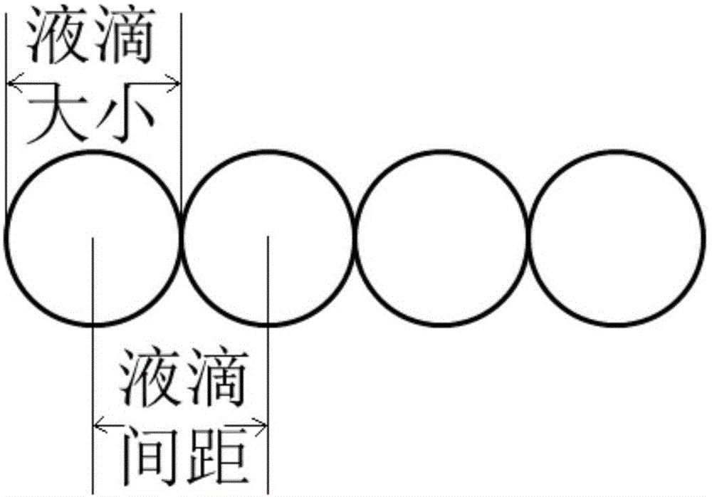
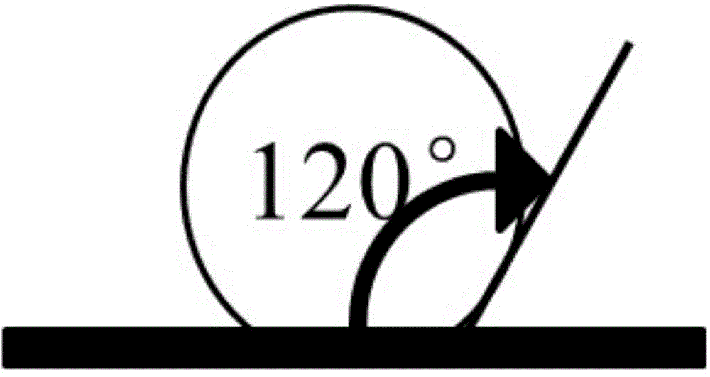
[0005] like Figure 2a , Figure 2b As shown, the surface of PDMS is extremely hydrophobic, resulting in a small droplet diameter, which cannot be dispersed on the substrate, which is not conducive to the evaporation of the droplet solvent, because the working speed of the jet printing system and the droplet distance (by Figure 2a , Figure 2b It can be seen that the smaller droplet diameter needs to be set smaller droplet spacing) is proportional to, so the hydrophobic characteristics of the PDMS surface lead to a longer processing time
[0006] like image 3 as shown, Figure 2a , Figure 2b The problem shown also leads to the formation of larger circular droplets due to surface tension mutual attraction and displacement between adjacent wet droplets, which makes the original printing area appear blank, which is not conducive to the formation of electrodes with better continuity

Method used


Image

  • Method for processing microelectrode on PDMS substrate based on inkjet printing technology
  • Method for processing microelectrode on PDMS substrate based on inkjet printing technology
  • Method for processing microelectrode on PDMS substrate based on inkjet printing technology

Examples


Embodiment Construction

[0042] The method for processing microelectrodes on a PDMS substrate based on the inkjet printing technology of the present invention will be described in detail below in conjunction with the embodiments and the accompanying drawings.

[0043]The method for processing microelectrodes on the PDMS substrate based on inkjet printing technology of the present invention adopts a model that is Dimatix 2831, Fujifilm, an inkjet printer capable of spraying silver nanoparticle solution of Japan, because the nozzle is printing the support rod The left and right movement of the upper body and the front and rear movement of the chassis, the silver nanoparticle droplets ejected from the nozzle can process the silver layer model of the two-dimensional structure. silver layer. Since the system prints according to the pre-designed image file, it only deposits silver nanoparticles where needed, no mask is required, and the processing process is efficient and simple.

[0044] The method for pr...


PUM

PropertyMeasurementUnit
thicknessaaaaaaaaaa

Abstract

The invention relates to a method for processing a microelectrode on a PDMS substrate based on an inkjet printing technology. The method comprises: preparing a PDMS substrate, wherein a PDMS monomer and a curing agent are uniformly mixed according to a mass ratio of 10:1, gas bubbles are removed, the PDMS mixed with the curing agent is poured onto the surface of a polished silicon wafer, and the obtained material is placed into a constant temperature oven for 2 h to cure; increasing adhesion of the PDMS on the metal electrode; and carrying out splitting and re-combination on the effective pixel part in the original electrode pattern by using a digital image treatment method, and then carrying out spray printing in a one-by-one manner according to the effective pixel in the new pattern. According to the present invention, the problem of poor electrode continuity caused by the surface tension of the liquid droplet is overcome, the hydrophobic property of the PDMS surface is improved, the processing efficiency is improved, and the poor adhesion of the silver electrode on the PDMS surface is solved; and the method has characteristics of high efficiency, convenience and high automation degree, and the processed electrode has characteristics of good PDMS surface adhesion and high quality.

Description

technical field [0001] The invention relates to a micro-electrode processed on PDMS. In particular, it involves a pixel-level jet printing method and the use of chemical coupling agent MPTMS to modify the surface of PDMS to improve its surface hydrophobicity and adhesion to silver electrodes. Processing microelectrodes on PDMS substrates based on inkjet printing technology Methods. Background technique [0002] Microfluidic chips based on PDMS (polydimethylsiloxane) have been widely used in biomacromolecule detection, electrochemical sensing, medical instrument manufacturing, and wearable devices. As a flexible material, PDMS is the material of choice for manufacturing integrated on-chip sensing systems due to its non-toxicity, transparency, ease of processing, and good biocompatibility. However, integrating microelectrodes in microfluidic channels to form functional biosensors is still a challenge in the scientific community, because processing microelectrodes on PDMS has...

Claims


Application Information

Patent Timeline
Patent Type & Authority Applications(China)
IPC IPC(8): G01N27/30B41J2/01
Inventor 栗大超吴建伟于海霞徐可欣
Owner TIANJIN UNIV
Learn More