Ion implantation method capable of preventing silicon edge on boundary of ion implantation region from peeling off

An ion implantation area, ion implantation technology, applied in the direction of electrical components, semiconductor/solid-state device manufacturing, circuits, etc., can solve the problems of silicon surface amorphization, silicon peeling, etc., to improve product yield, reduce surface defects, strong The effect of process compatibility

Active Publication Date: 2015-10-14
西安西岳电子技术有限公司
View PDF5 Cites 1 Cited by
  • Summary
  • Abstract
  • Description
  • Claims
  • Application Information

AI Technical Summary

Problems solved by technology

High energy (above 80KeV) large dose (1E15ions / cm 2 The above) ion implantation will lead to the amorphization of the silicon surface layer. During the subsequent degelling process, the boundary of the amorphous layer in the implanted area will generate protruding fine edges due to stress, and the silicon will peel off due to the interaction with the photoresist.

Method used


Image

  • Ion implantation method capable of preventing silicon edge on boundary of ion implantation region from peeling off
  • Ion implantation method capable of preventing silicon edge on boundary of ion implantation region from peeling off
  • Ion implantation method capable of preventing silicon edge on boundary of ion implantation region from peeling off

Examples


Embodiment 1

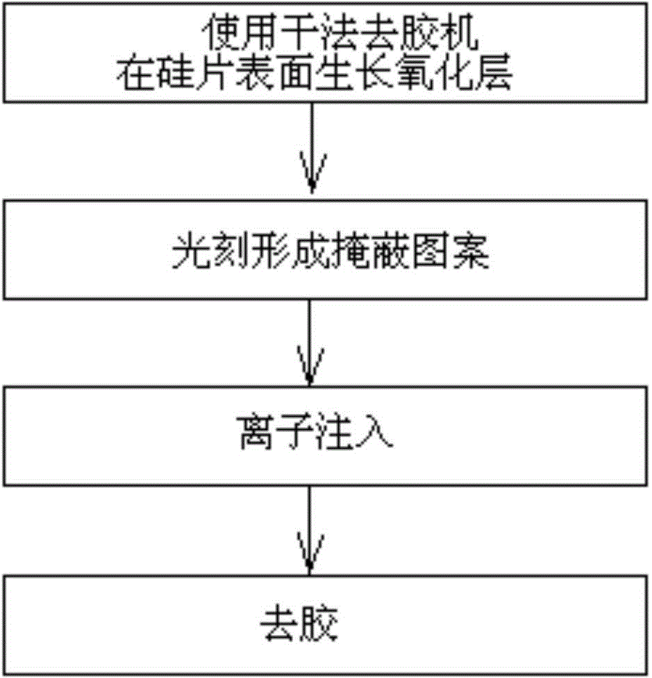
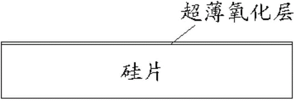
[0042] Step 1: Use a dry degumming machine to treat the surface of the silicon wafer. The specific method is: use a lamp to illuminate the silicon wafer to 180°C, and the illumination time is 20s. During the whole process, O 2 , pass into O 2 The flow rate is 6SLPM, O 2 The air pressure is 4.5Torr, so that the surface growth thickness of the silicon wafer is the oxide layer;

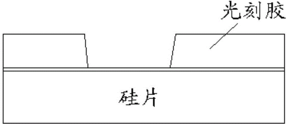
[0043] Step 2: Coating thickness on the silicon wafer treated in step 1 is photoresist;

[0044] Step 3: Perform ion implantation on the silicon wafer treated in step 2, the implantation energy is 80KeV during ion implantation, and the implantation dose of arsenic is 1E15ions / cm 2 ;

[0045] Step 4: firstly remove the photoresist on the surface of the silicon wafer by using the plasma dry method to remove the glue, and then use the wet method to remove the glue.

Embodiment 2

[0047] Step 1: Use a dry degumming machine to treat the surface of the silicon wafer. The specific method is: use a lamp to illuminate the silicon wafer to 220°C, and the illumination time is 40s. During the whole process, O 2 , pass into O 2 The flow rate is 4SLPM, O 2 The air pressure is 3.5Torr, so that the surface growth thickness of the silicon wafer is the oxide layer;

[0048] Step 2: Coating thickness on the silicon wafer treated in step 1 is photoresist;

[0049] Step 3: Perform ion implantation on the silicon wafer treated in step 2, the implantation energy is 160KeV during ion implantation, and the implantation dose of phosphorus is 4E15ions / cm 2 ;

[0050] Step 4: Removing the photoresist on the surface of the silicon wafer by means of dry stripping and wet stripping.

Embodiment 3

[0052] Step 1: Use a dry degumming machine to treat the surface of the silicon wafer. The specific method is: use a lamp to illuminate the silicon wafer to 200°C, and the illumination time is 30s. During the whole process, O 2 , pass into O 2 The flow rate is 5SLPM, O 2 The air pressure is 4Torr, so that the surface growth thickness of the silicon wafer is the oxide layer;

[0053] Step 2: Coating thickness on the silicon wafer treated in step 1 is photoresist;

[0054] Step 3: Perform ion implantation on the silicon wafer treated in step 2, the implantation energy is 120KeV during ion implantation, implant arsenic and the implantation dose is 6E15ions / cm 2 ;

[0055] Step 4: Removing the photoresist on the surface of the silicon wafer by means of dry stripping and wet stripping.


PUM


Abstract

The present invention discloses an ion implantation method capable of preventing a silicon edge on the boundary of an ion implantation region from peeling off. The method comprises the following steps of: firstly, performing processing on the surface of a silicon chip, so that an oxide layer is generated on the surface of the silicon chip; then coating the silicon chip with a photoresist; then performing ion implantation on the silicon chip; and finally removing the photoresist on the surface of the silicon chip. According to the present invention, by performing processing on the surface of the silicon chip, an ultrathin oxide layer is generated on the surface of the silicon chip to prevent the silicon chip from generating the silicon edge in the photoresist-removing process, thereby avoiding the silicon peeling problem, reducing surface defects and improving the rate of finished products.

Description

technical field [0001] The invention belongs to the technical field of semiconductor manufacturing, and in particular relates to an ion implantation method capable of preventing silicon ribs from peeling off at the boundary of an ion implantation region. Background technique [0002] The N-type doping of electrostatic (ESD) protection devices in MOS circuits uses bare silicon surface, which is implanted with high-energy and large-dose arsenic or phosphorus to form ohmic contacts. High energy (above 80KeV) large dose (1E15ions / cm 2 The above) ion implantation will lead to amorphization of the silicon surface layer. During the subsequent degelling process, protruding thin ribs will be generated at the boundary of the amorphous layer in the implanted area due to stress, and the silicon will peel off due to the interaction with the photoresist. For example, a large dose of arsenic or phosphorus implantation will damage the silicon lattice on the surface of the silicon wafer and...

Claims


Application Information

Patent Timeline
Patent Type & Authority Applications(China)
IPC IPC(8): H01L21/266
CPCH01L21/266
Inventor 李宁付鹏张思申利阳汪小军
Owner 西安西岳电子技术有限公司
Why Eureka
Try Eureka