Flexible organic light emission diode and preparation method thereof
An electroluminescent device and electroluminescent technology, which are applied in the fields of electric solid state devices, semiconductor/solid state device manufacturing, electrical components, etc., and can solve problems such as cracks in inorganic thin films, peeling off of stainless steel substrates, and damage to light-emitting devices.
- Summary
- Abstract
- Description
- Claims
- Application Information
AI Technical Summary
Problems solved by technology
Method used
Image
Examples
preparation example Construction
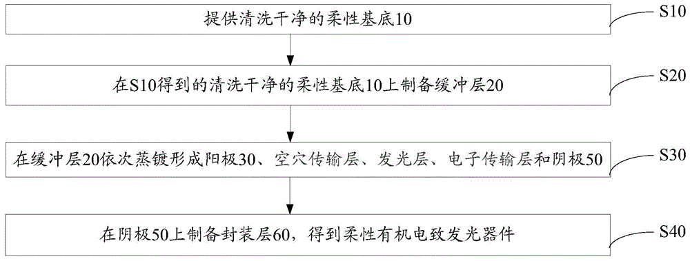
[0051] Such as figure 2 The preparation method of the above-mentioned flexible organic electroluminescent device shown includes the following steps:
[0052] S10 , providing a cleaned flexible substrate 10 .
[0053] The flexible substrate 10 can be a thin stainless steel sheet with a thickness of 0.05mm-0.2mm and a surface roughness (Ra) of less than 0.6μm.
[0054] Clean the stainless steel sheet for use.
[0055] S20 , preparing a buffer layer 20 on the cleaned flexible substrate 10 obtained in S10 .
[0056] The buffer layer 20 is an organic buffer film and an inorganic buffer film alternately laminated three to five times.
[0057] The material of the organic buffer film is copper phthalocyanine (CuPc), zinc phthalocyanine (ZnPc) or platinum phthalocyanine (PtPc), and the material of the inorganic buffer film is silicon dioxide or aluminum oxide.
[0058] In S20, the vacuum degree is 1×10 -5 ~1×10 -3 Pa.
[0059] The organic buffer film is prepared by thermal resi...
Embodiment 1
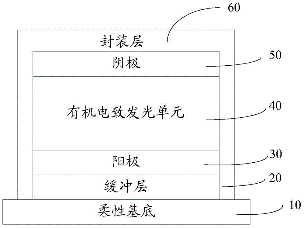
[0084] A flexible organic electroluminescent device, including a flexible substrate, a buffer layer, an anode, a hole transport layer, a light emitting layer, an electron transport layer, a cathode and an encapsulation layer stacked in sequence, and the specific structure is expressed as: stainless steel sheet / CuPc / Al 2 o 3 / CuPc / Al 2 o 3 / CuPc / Al 2 o 3 / CuPc / Al 2 o 3 / CuPc / Al 2 o 3 / Ag / NPB / Rubrene / Alq 3 / Al / CuPc / Al 2 o 3 / CuPc / Al 2 o 3 / CuPc / Al 2 o 3 / CuPc / Al 2 o 3 / CuPc / Al 2 o 3 .
[0085] The preparation steps are:
[0086] A stainless steel sheet with a thickness of 0.05mm is provided, cleaned and ready for use.
[0087] In a vacuum of 1×10 -5 In the vacuum coating system of Pa, the CuPc film was prepared by thermal resistance evaporation on the surface of the stainless steel sheet at an evaporation rate of 0.5nm / s, and then Al was prepared on the surface of the CuPc film by electron beam evaporation at an evaporation rate of 0.5nm / s. 2 o 3 film. Re...
Embodiment 2
[0095] A flexible organic electroluminescent device, including a flexible substrate, a buffer layer, an anode, a hole transport layer, a light emitting layer, an electron transport layer, a cathode and an encapsulation layer stacked in sequence, the specific structure is expressed as: stainless steel sheet / ZnPc / SiO 2 / ZnPc / SiO 2 / ZnPc / SiO 2 / Al / m-MTDATA / DPVBi / Bphen / Ag / ZnPc / SiO 2 / ZnPc / SiO 2 / ZnPc / SiO 2 .
[0096] The preparation steps are:
[0097] A stainless steel sheet with a thickness of 0.2mm is provided, cleaned and ready for use.
[0098] In a vacuum of 1×10 -3 In the vacuum coating system of Pa, the ZnPc film was prepared by thermal resistance evaporation on the surface of the stainless steel sheet at an evaporation rate of 1nm / s, and then SiO was prepared on the surface of the ZnPc film by electron beam evaporation at an evaporation rate of 2nm / s. 2 film. Repeat for ZnPc films and SiO 2 The preparation process of the film, the preparation of a total of 3 laye...
PUM
| Property | Measurement | Unit |
|---|---|---|
| Thickness | aaaaa | aaaaa |
| Thickness | aaaaa | aaaaa |
| Thickness | aaaaa | aaaaa |
Abstract
Description
Claims
Application Information

