
Light emitting diode packaging structure

A technology of light-emitting diodes and packaging structures, applied in the direction of electrical components, circuits, semiconductor devices, etc., can solve the problems of unfavorable light emitting upward, affecting light extraction efficiency, unfavorable integration, etc., to achieve concentrated color point output, high light efficiency, Production cost reduction effect

Active Publication Date: 2015-10-28
XIAMEN SANAN OPTOELECTRONICS TECH CO LTD
View PDF8 Cites 27 Cited by
  • Summary
  • Abstract
  • Description
  • Claims
  • Application Information

AI Technical Summary

Problems solved by technology

However, there are the following disadvantages: (1) The packaging structure needs to be installed on a ceramic substrate, which is large in size, which is not conducive to integration; (2) The glue wall is vertical, which is not conducive to the upward emission of light, which affects the light extraction efficiency

Method used


Image

  • Light emitting diode packaging structure
  • Light emitting diode packaging structure
  • Light emitting diode packaging structure

Examples


Embodiment 1

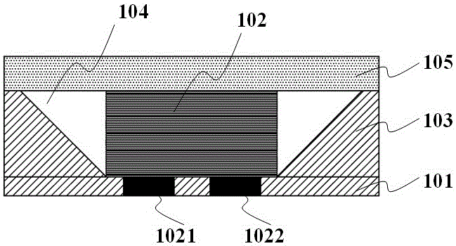
[0055] like figure 1As shown, this embodiment discloses a light emitting diode packaging structure, which is composed of a flip chip 102 , a first reflective material layer 101 , a second reflective material layer 103 , a first transparent material layer 104 and a wavelength conversion material layer 105 .

[0056] Wherein the flip chip 102 is located on the first reflective material layer 101 having a through hole, and the electrode 1021 and the electrode 1022 of the flip chip 102 are embedded in the through hole of the first reflective material layer 101, that is, the side surface of the electrode or Part of the side surface is surrounded by the first reflective material layer 101 . The positive and negative electrodes ( 1021 and 1022 ) of the flip chip 102 contain one of metal copper or gold, and the thickness thereof is between 10 μm and 100 μm. The first light-reflecting material layer 101 and the thicker electrodes can relieve the stress of the PCB on the flip-chip when...

Embodiment 2

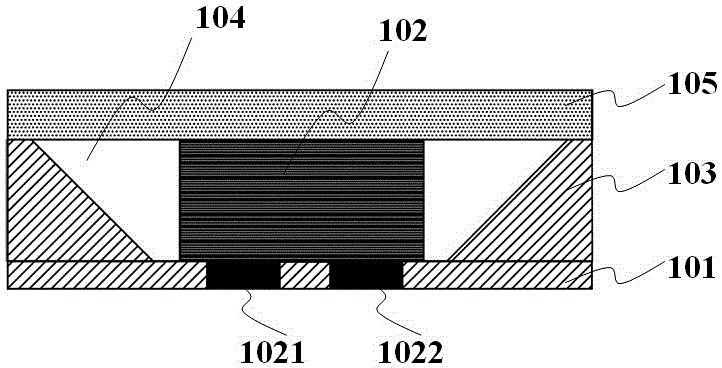
[0060] Such as figure 2 As shown, compared with Embodiment 1, there is a certain distance between the inner edge of the bottom of the second light-reflecting material layer 103 of this embodiment and the side surface of the flip chip 102, so that the size of the flip chip can be kept constant. Increase the light-emitting area, and improve the light efficiency to a certain extent.

Embodiment 3

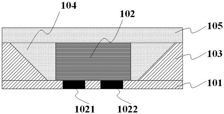
[0062] Such as image 3 As shown, compared with Embodiment 1, the first transparent material layer 104 of this embodiment contains a wavelength conversion material. For example, a red light conversion material is added to the first transparent material layer, and only yellow light or green light conversion material is contained in the wavelength conversion material layer 105, so as to avoid the secondary absorption of yellow light or green light by the red light conversion material, which can effectively Improve light efficiency.


PUM

PropertyMeasurementUnit
Thicknessaaaaaaaaaa
Thicknessaaaaaaaaaa

Abstract

The invention discloses a light emitting diode packaging structure. The light emitting diode packaging structure is characterized in that the packaging structure comprises a first light reflection material layer with through holes, an inverted chip located on the first light reflection material layer, a first transparent material layer surrounding the side surface, except the electrodes, of the inverted chip and a second light reflection material layer surrounding the first transparent material layer. Electrodes of the inverted chip are inlaid in the through holes of the first light reflection material layer. The interface surface of the first transparent material layer and the light reflection material layer is an inclined plane or a cambered surface or an irregular shape, which facilitates light of the inverted chip to reflect upwards. A wavelength conversion material layer covers the above structure.

Description

technical field [0001] The invention relates to a packaging structure, in particular to a light emitting diode packaging structure. Background technique [0002] Light Emitting Diode (English for Light Emitting Diode, referred to as LED) is a semiconductor light emitting device made of the principle of P-N junction electroluminescence of semiconductors. LED has the advantages of environmental protection, high brightness, low power consumption, long life, low working voltage, and easy integration. It is the fourth-generation new light source after incandescent lamps, fluorescent lamps and high-intensity discharge (HID) lamps. [0003] The traditional LED packaging structure consists of die bonding, wire bonding, and fluorescent glue sealing on a metal bracket. Recently, the use of flip-chip level packaging is very popular. This kind of packaging does not use a substrate or wire bonding. It can directly cover the chip with fluorescent glue and then cut it. It has a large lum...

Claims


Application Information

Patent Timeline
IPC IPC(8): H01L33/48H01L33/60
CPCH01L33/483H01L33/60
Inventor 徐宸科时军朋蔡培崧林振端黄昊廖晨杰赵志伟
Owner XIAMEN SANAN OPTOELECTRONICS TECH CO LTD
Learn More