Eureka AIR delivers breakthrough ideas for toughest innovation challenges, trusted by R&D personnel around the world.

Graphene electro-optic modulation device based on photonic crystal nanometer beam resonant cavity

An electro-optic modulation and photonic crystal technology, applied in optics, nonlinear optics, instruments, etc., can solve problems such as limited MRR, increased bending loss, and reduced modulation efficiency, achieving high-speed power consumption, low power consumption, and favorable The effect of large-scale integrated development

Inactive Publication Date: 2015-11-11
SHANGHAI JIAO TONG UNIV
View PDF4 Cites 13 Cited by
  • Summary
  • Abstract
  • Description
  • Claims
  • Application Information

AI Technical Summary

Problems solved by technology

Compared with the straight waveguide structure, the micro-ring resonant structure increases the length of interaction between light and graphene and greatly increases the modulation depth, but the MRR is limited by the free spectral range FSR. While reducing the ring radius to increase the FSR Will increase bending loss and reduce modulation efficiency

Method used


Image

  • Graphene electro-optic modulation device based on photonic crystal nanometer beam resonant cavity
  • Graphene electro-optic modulation device based on photonic crystal nanometer beam resonant cavity
  • Graphene electro-optic modulation device based on photonic crystal nanometer beam resonant cavity

Examples


Embodiment 1

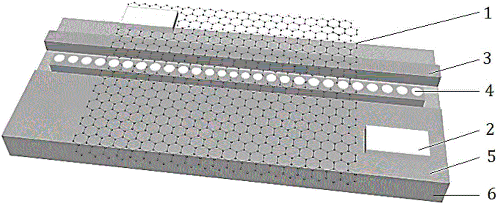
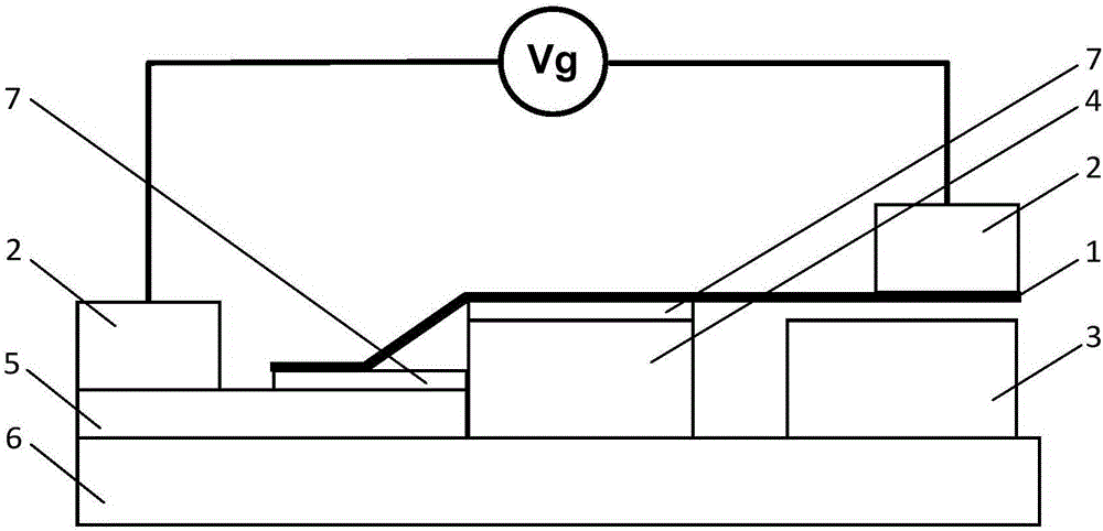
[0032] Such as figure 1 with figure 2 As shown, this embodiment includes: a pair of electrodes 2, a graphene layer 1, an SOI substrate 6, an optical coupling waveguide 3, a PCNC4, and an N-type silicon-doped region 5 arranged side by side on the SOI substrate 6, wherein: the graphene layer 1 is arranged above the optical coupling waveguide 3, PCNC4 and the N-type silicon-doped region 5, and two electrodes are respectively arranged on the N-type silicon-doped region 5 and the graphene layer 1 above the optical coupling waveguide 3.

[0033] The N-type silicon-doped region 5 is connected to the graphene layer 1 through an aluminum oxide isolation layer 7 .

[0034] The thickness of silicon on top of the SOI substrate 6 is 220 nm, and a silicon dioxide buffer layer with a thickness of 2 μm is arranged in the middle.

[0035] The top silicon patterning of the SOI substrate 6 is accomplished by 248nm deep ultraviolet lithography and ion coupled etching (ICP).

[0036] The N-typ...


PUM

PropertyMeasurementUnit
thicknessaaaaaaaaaa
thicknessaaaaaaaaaa
thicknessaaaaaaaaaa

Abstract

A graphene electro-optic modulation device based on a photonic crystal nanometer beam resonant cavity comprises a pair of electrodes, a graphene layer, an SOI substrate, an optical coupling waveguide, an PCNC and an N type silicon doping area, wherein the optical coupling waveguide, the PCNC and the N type silicon doping area are sequentially arranged on the SOI substrate in parallel, the graphene layer is arranged on the optical coupling waveguide, the PCNC and the N type silicon doping area, and the two electrodes are arranged at the portions, on the N type silicon doping area and the optical coupling waveguide, of the graphene layer respectively. The material advantages of broadband absorption of graphene, high mobility of carriers and the like and the structure advantages of small size and large FSR of the PCNC are integrated, the problem that in a current micro-ring resonant cavity graphene modulation device, FSR and size change in opposite ways is solved, the good modulation performance is achieved, and wide application prospects are achieved in optical fiber communication and optical interconnection systems.

Description

technical field [0001] The invention relates to a technology in the field of microwave communication, in particular to a graphene electro-optic modulation device based on a photonic crystal nanobeam cavity (Photomiccrystalnanobeamcavity, PCNC). Background technique [0002] Electro-optic modulation devices are key functional components in future optical signal processing and computing systems. Exploring high-speed, wide-bandwidth, and small-volume integrated electro-optic modulation devices for the interconnection of optical devices on chips is the development trend of modulation devices. Finding a material that is compatible with complementary metal-oxide-semiconductor (CMOS) technology, has good stability and reliability, and has sufficient modulation rate and modulation efficiency has become an important research content for scientists. [0003] The emergence of graphene has brought new opportunities and challenges to this research field. Graphene is a two-dimensional cr...

Claims


Application Information

Patent Timeline
Patent Type & Authority Applications(China)
IPC IPC(8): G02F1/035
CPCG02F1/035G02F2202/32
Inventor 潘听邱辞源吴佳旸周换颖苏翼凯
Owner SHANGHAI JIAO TONG UNIV
Why Eureka
Eureka Blog
Learn More