A visible near-infrared ultra-broadband absorber and its preparation method

a near-infrared and absorber technology, applied in the field of visible near-infrared ultra-broadband absorbers, can solve the problems of unsatisfactory absorption, complex preparation methods, high cost, etc., and achieve the effects of wide absorption band, good incidence angle insensitivity, and improved absorption performan

Active Publication Date: 2017-08-24
ZHEJIANG UNIV
View PDF0 Cites 6 Cited by
  • Summary
  • Abstract
  • Description
  • Claims
  • Application Information

AI Technical Summary

Benefits of technology

[0008]The present invention is related to a visible near-infrared ultra-broadband absorber which has wider absorption band, better absorption performance and good incidence angle insensitivity.
[0009]The present invention further provides a preparation method for the visible near-infrared ultra-broadband absorber with convenient preparation and low cost, and thus is suitable for large-scale mass production.
[0023]Compared with the traditional absorbers, the visible near-infrared ultra-broadband absorber of the present invention has wider absorption band, better absorption performance and good incidence angle insensitivity. Therefore, the visible near-infrared broadband absorber of the present invention has fully surpassed traditional absorbers. Since the visible near-infrared broadband absorber of the present invention has a compact multilayer film structure that is simpler compared with the conventional broadband absorbers and artificial electromagnetic absorbers proposed in recent years. Owing to such compact multilayer film structure, the visible near-infrared broadband absorber of the present invention has avoided such complicated nano-fabrication techniques as electron beam machining technique, focused ion beam etching technique, reaction ion etching technique and lithography. Therefore, it can significantly reduce production cost and shorten the production cycle, which is convenient for large-scale mass production.
[0024]The present invention has established a broadband opaque anti-reflection structure based on blocking effect of the metal absorbing layer and broadband anti-reflection film stack on the germanium layer; therefore, it has realized visible near-infrared ultra-broadband absorption with high efficiency and angle insensitivity. The visible near-infrared ultra-broadband absorber in the present invention has simple structure, conveneint preparation and low cost, which is suitable for large-scale mass production, so that the preparation cost of the visible near-infrared ultra-broadband absorber has been significantly reduced. Therefore, the present invention is expected to have an extensive application in photo-thermal conversion, electromagnetic absorption, exploration and imaging so as to make great contribution to China's national economy, social development, science and technology, national defense construction and other fields.

Problems solved by technology

However, the aforesaid preparation methods are complicated and time-consuming with high cost, and thus are not suitable for large-scale mass production.
The structure is relatively simple but its absorption is unsatisfactory.
The absorption of the coating below 0.9 and the preparation process is complicated.

Method used


Image

  • A visible near-infrared ultra-broadband absorber and its preparation method
  • A visible near-infrared ultra-broadband absorber and its preparation method
  • A visible near-infrared ultra-broadband absorber and its preparation method

Examples


embodiment 1

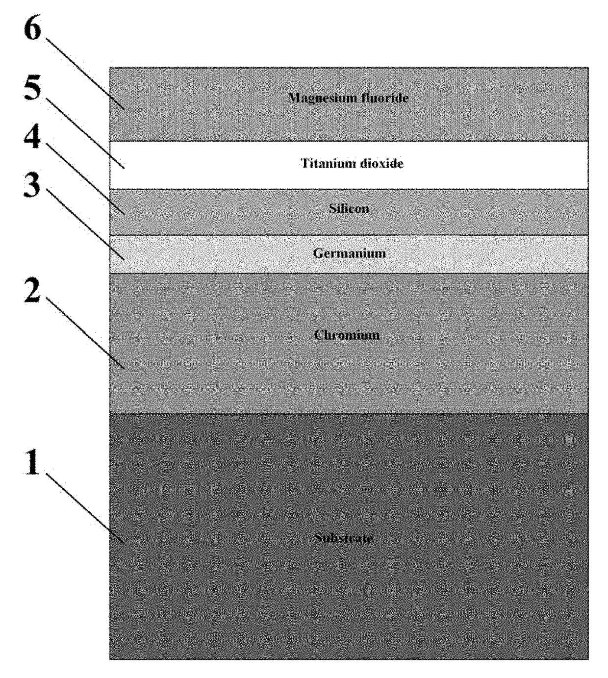
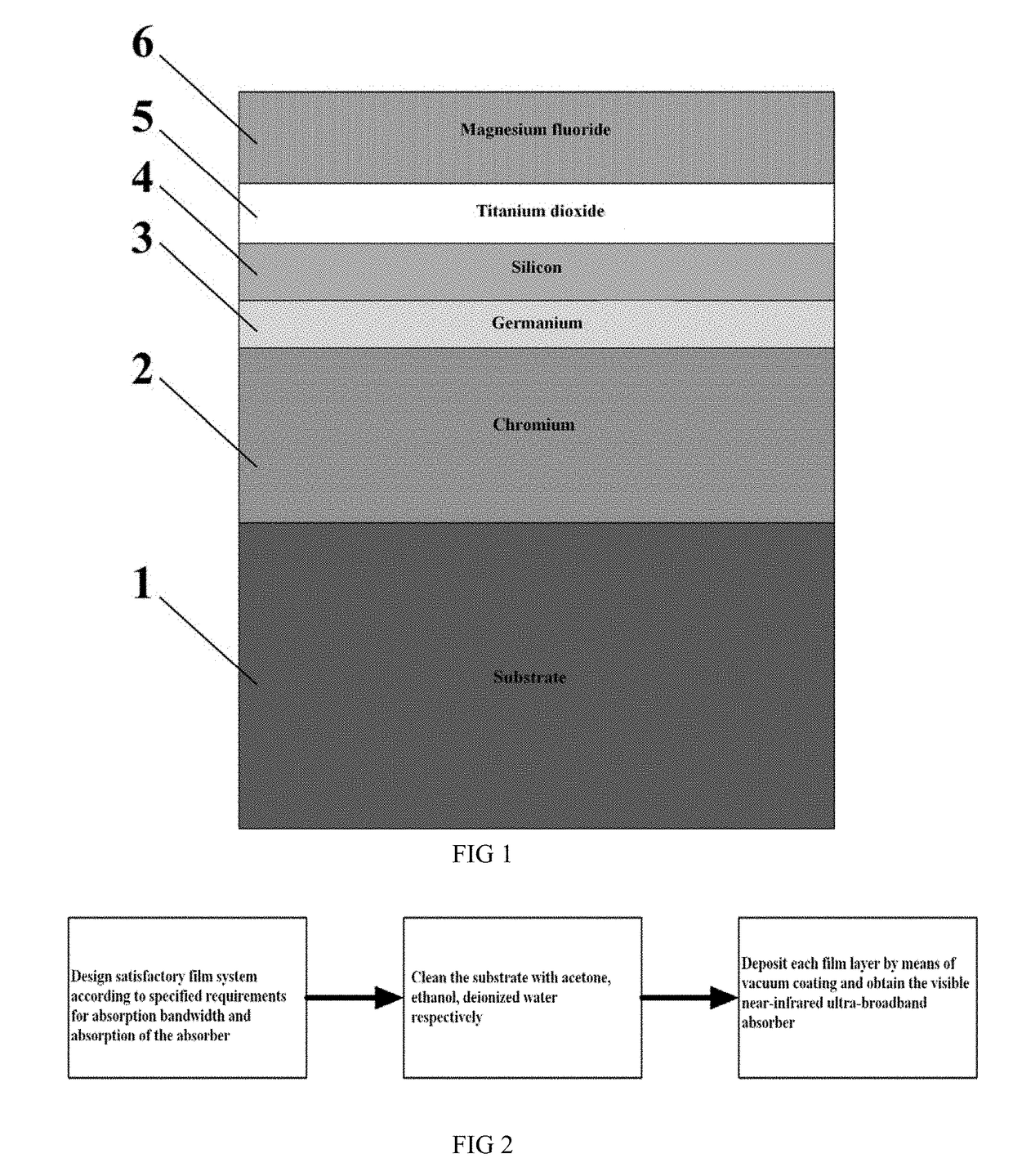
[0050]The visible near-infrared ultra-broadband absorber has the anticipated absorption bandwidth of 400 nm-1200 nm with average absorption rate over 98%; the absorption spectrum of the designed and prepared absorber sample of the present invention is as shown in FIG. 4(a) with average absorption rate over 98.75%; corresponding substrate material is silicon and material of corresponding film layer is chromium, germanium, silicon, titanium dioxide and magnesium fluoride respectively with a thickness of 200 nm (chromium), 18 nm (germanium), 19 nm (silicon), 35 nm (titanium dioxide) and 80 nm (magnesium fluoride) respectively.

embodiment 2

[0051]The visible near-infrared ultra-broadband absorber has the anticipated absorption bandwidth of 400 nm-2000 nm with absorption rate per wavelength over 90%; the absorption spectrum of the designed and prepared absorber sample of the present invention is as shown in FIG. 4(b) with average absorption rate over 97.75%; corresponding substrate material is silicon and material of corresponding film layer is chromium, germanium, silicon, titanium dioxide and magnesium fluoride respectively and a thickness 200 nm (chromium), 33 nm (germanium), 32 nm (silicon), 56 nm (titanium dioxide) and 118 nm (magnesium fluoride) respectively.

embodiment 3

[0052]It is basically identical to Embodiment 1; the only difference is that chromium is replaced by titanium and other conditions are identical to Embodiment 1; the designed absorption spectrum of the present invention is as shown in FIG. 4 (c) with average absorption rate over 99% and thickness of corresponding film layer of 200 nm (titanium), 12 nm (germanium), 17 nm (silicon), 38 nm (titanium dioxide) and 89 nm (magnesium fluoride) respectively.


PUM

PropertyMeasurementUnit
thicknessaaaaaaaaaa
thicknessaaaaaaaaaa
thicknessaaaaaaaaaa

Abstract

The present invention discloses a visible near-infrared ultra-broadband absorber and its preparation method, comprising a substrate and a five-layer optical film, wherein the bottom film is a bottom metal absorbing layer; a top germanium layer is provided on the top of the bottom metal absorbing layer; and remaining three layers are provided on the top of the top germanium layer with gradually decreasing refractive indexes from the bottom to the top. The present invention is based on the blocking effect of the metal absorbing layer and broadband anti-reflection film stack of the germanium layer, which has realized visible near-infrared ultra-broadband absorption with high efficiency and good angle insensitivity, and has fully surpassed traditional absorbers in terms of performances. Compared with conventional broadband absorbers and artificial electromagnetic absorbers proposed in recent years, the compact multilayer film structure in the present invention is simpler and avoides complicated nano-fabrication techniques. Therefore, it can significantly reduce production cost and shorten the production cycle, and is thus suitable for large-scale mass production.

Description

FIELD OF THE INVENTION[0001]The present invention is related to such fields as elimination of stray light, space exploration, imaging, photo-thermal conversion and electromagnetic absorption, in particular to a visible near-infrared ultra-broadband absorber.BACKGROUND OF THE INVENTION[0002]As the visible near-infrared broadband absorber plays an important role in numerous different new fields, more and more ultra-broadband absorbers have been developed in recent years based on extensive study. In recent years, researchers have proposed various near-infrared electromagnetic wave absorbers with artificial electromagnetic structure. Among them, Chen et al. have produced gold nanorod in random arrangement on the metal substrate coated with a dielectric layer by means of droplet evaporation, and thereby realized high absorption at the near-infrared broadband of 900 nm-1600 nm (Near-infrared broadband absorber with film-coupled multilayer nanorods, Optics Lett. 38, 2247-2249 (2013)); Zhou...

Claims


Application Information

Patent Timeline
Patent Type & Authority Applications(United States)
IPC IPC(8): G02B5/00G02B1/115
CPCG02B1/115G02B5/003B32B9/00B32B15/00
Inventor SHEN, WEIDONGYANG, CHENYINGZHANG, YUEGUANGFANG, BOLIU, XU
Owner ZHEJIANG UNIV
Why Eureka
Try Eureka