No-board-edge nickel-gold technology of circuit board

A circuit board and process technology, which is applied in the field of circuit board edgeless nickel-gold process, can solve the problems of chemical nickel wire pollution, raw material and labor waste, etc., and achieve the effect of saving consumption and ensuring direction positioning

Inactive Publication Date: 2015-11-18
湖北建浩科技有限公司
View PDF4 Cites 2 Cited by
  • Summary
  • Abstract
  • Description
  • Claims
  • Application Information

AI Technical Summary

Problems solved by technology

The current method has the following disadvantages: hemming and ink coating cause waste of raw materials and labor; the tape and ink have the risk of falling off and causing the chemical nickel wire to be polluted under the corrosion of the chemical nickel gold solution;

Method used


Image

  • No-board-edge nickel-gold technology of circuit board
  • No-board-edge nickel-gold technology of circuit board

Examples


Embodiment Construction

[0018] Describe below in conjunction with accompanying drawing and specific embodiment:

[0019] A circuit board edgeless nickel-gold process, comprising:

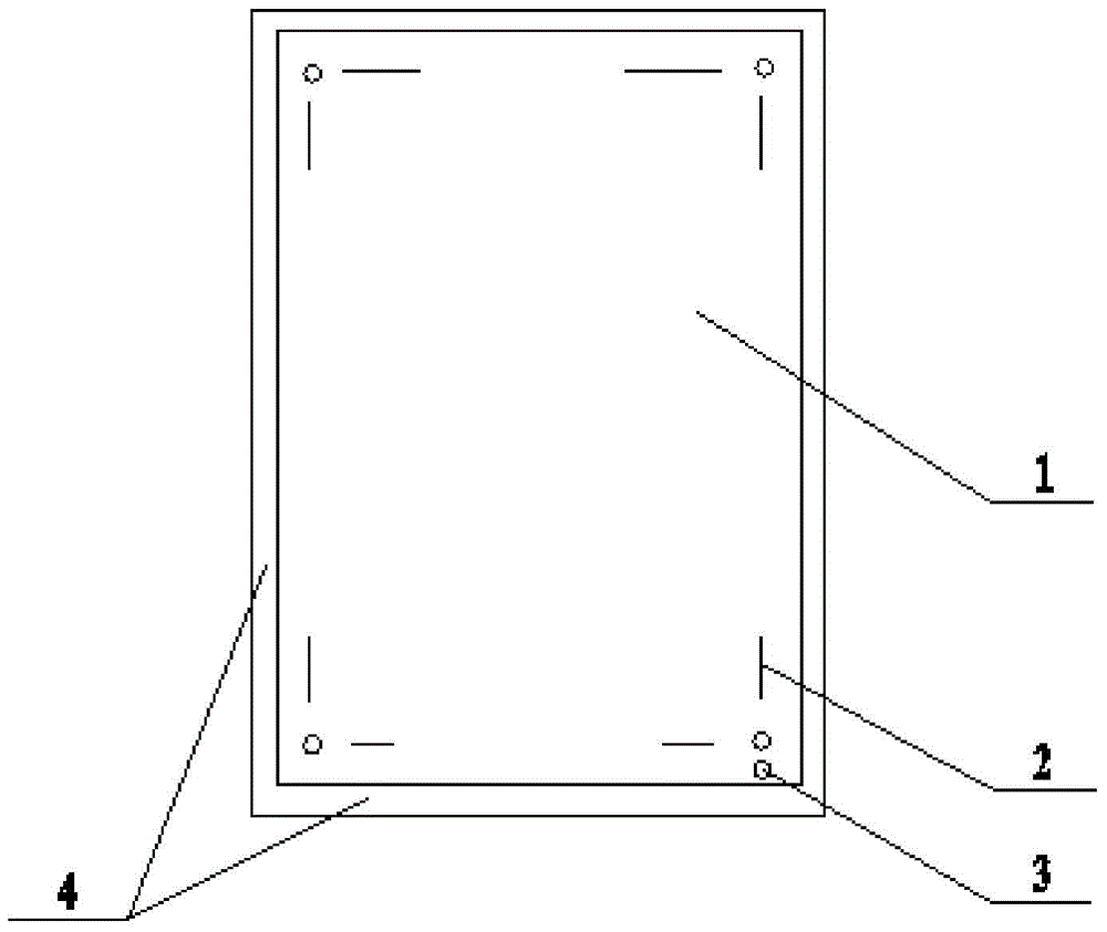
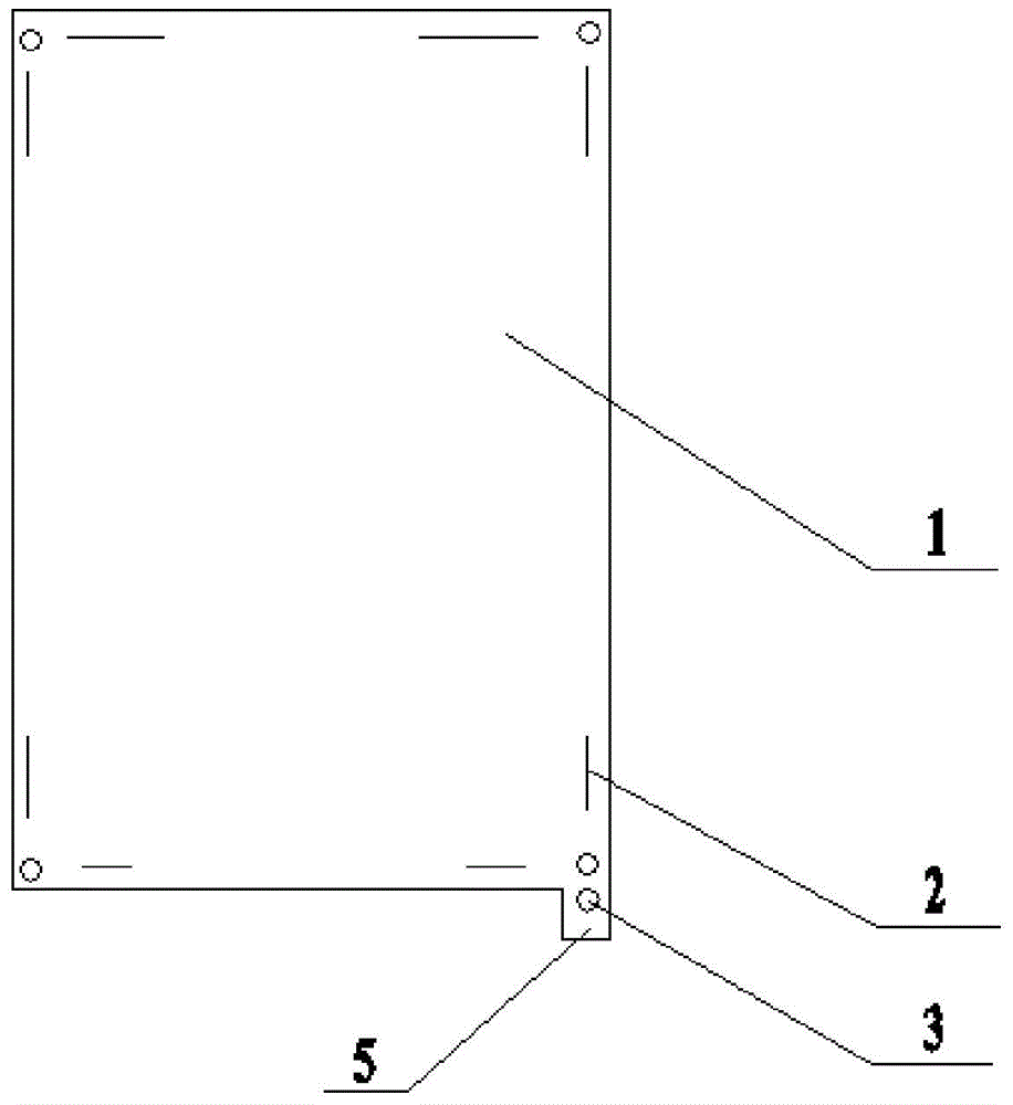
[0020] S1. Cutting the circuit board 1 substrate (plate type: FR-4TG140A grade plate, length 622mm, width 435mm, plate thickness 1.5mm, copper thickness 1 / 1OZ, the width of the reserved process side 4 is 10.2mm in the width direction , length direction 13.48mm), drilling (Shenzhen Han’s drilling machine, spindle speed 200,000 rpm, drill tape P02E57032A0.drl, minimum aperture 0.4mm), after electroless copper deposition, use a 50 times microscope to observe the backlight level as Level 9; followed by whole board electroplating, current density 15ASF, electroplating time 30min;

[0021] S2. After the pretreatment of the dry film on the electroplated circuit board, paste the dry film in the clean room (Changxing dry film HT-115T21.00inch, 600ft, film pressure 3.8kg / cm 2 , film temperature 110°C), after film application, let ...


PUM


Abstract

The invention discloses a no-board-edge nickel-gold technology of a circuit board. The no-board-edge nickel-gold technology of a circuit board comprises steps of performing cutting on a substrate of the circuit board, exposing an inner layer circuit, laminating, boring, precipitating copper and electroplating, adopting a positive technology to perform copper plating, tin plating, removing films, etching, removing tin, performing solder mask, and performing character back baking on the outer layer circuit. The steps before the chemical nickel-gold technology comprises steps of removing the technology edges on the circuit board, performing chemical nickel-gold processing on the circuit board, and testing and checking the electric performance and appearance of the finished board. The invention can save the nickel amount in the nickel gold technology so as to save the cost.

Description

technical field [0001] The invention relates to a method for plating gold on a circuit board, in particular to a nickel-gold process without edge of the circuit board. Background technique [0002] PCB board is a circuit board made by electronic printing technology for making electronic components. The manufacturing process of PCB board is complicated and the process is long, generally including cutting-drilling-copper sinking-full board electroplating-graphic transfer-graphics Electroplating copper nickel gold-etching-inspection and other processes, in which nickel and gold plating on the copper foil surface of the conductive pattern on the printed circuit board is a very important step, which can effectively prevent copper migration and oxidation, and improve the conductivity of the PCB board and antioxidant properties. In the traditional electro-nickel-gold process of printed circuit boards, in the process of PCB electroplating, for normal electroplating and silk screen ...

Claims


Application Information

Patent Timeline
Patent Type & Authority Applications(China)
IPC IPC(8): H05K3/24
CPCH05K3/241
Inventor 蔡仁凯
Owner 湖北建浩科技有限公司
Why Eureka
Try Eureka