Preparation method of three-dimensional honeycomb CuInS2 nanowire array solar absorbing material

A nanowire array and solar energy absorption technology, which is applied in the field of solar energy applications, can solve the problems of limited application space, difficulty comparable to array structures, and inability to obtain two-dimensional layered structures, etc., to achieve good light harvesting ability, improved band gap, and uniformity good sex effect

Active Publication Date: 2015-11-25
SHANGHAI JIAO TONG UNIV
View PDF6 Cites 0 Cited by
  • Summary
  • Abstract
  • Description
  • Claims
  • Application Information

AI Technical Summary

Problems solved by technology

Since the patent chooses cuprous oxide powder as the self-sacrificing template, the obtained CuInS 2 It is a powdery hollow nanomaterial, which is difficult to match the advantages of the array structure, which limits its application space
In addition, the method adopted in this patent cannot obtain the two-dimensional layered CuInS 2

Method used


Image

  • Preparation method of three-dimensional honeycomb CuInS2 nanowire array solar absorbing material
  • Preparation method of three-dimensional honeycomb CuInS2 nanowire array solar absorbing material
  • Preparation method of three-dimensional honeycomb CuInS2 nanowire array solar absorbing material

Examples


Embodiment 1

[0029] A three-dimensional honeycomb CuInS 2 A method for preparing a nanowire array solar energy absorbing material, comprising the following steps:

[0030] (1) Mix indium chloride and thioacetamide at a molar ratio of 1:1 and add them to a polytetrafluoroethylene reactor, then add ethylene glycol to make a solution with an indium salt concentration of 0.5M, stir or ultrasonically dissolve ;

[0031] (2) placing the copper substrate for growing cuprous sulfide nanowire arrays in the reaction kettle;

[0032] (3) Seal the reactor, control the temperature at 200°C, and react for 4 hours; after the reaction, the reactor is naturally cooled to room temperature to obtain a three-dimensional honeycomb CuInS 2 The nanowire array film is uniformly grown on the surface of the copper substrate.

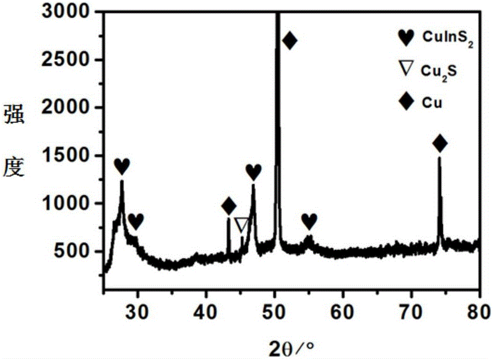
[0033] figure 1 For the CuInS obtained in this embodiment 2 XRD pattern of the film; by figure 1 It can be seen that, except for the peak of copper substrate, almost all peaks correspon...

Embodiment 2

[0037] A three-dimensional honeycomb CuInS 2 A method for preparing a nanowire array solar energy absorbing material, comprising the following steps:

[0038] (1) Mix indium acetate and thiourea at a molar ratio of 1:5 and add them to a polytetrafluoroethylene reactor, then add ethylene glycol to form a solution with an indium salt concentration of 0.2M, stir or ultrasonically dissolve;

[0039] (2) Place the bottom of the copper sheet growing the cuprous oxide nanowire array in the above-mentioned reaction kettle;

[0040] (3) Seal the reactor, control the temperature at 180°C, and react for 7 hours; after the reaction, the reactor is naturally cooled to room temperature to obtain a three-dimensional honeycomb CuInS 2 The nanowire array film is uniformly grown on the surface of the copper substrate.

Embodiment 3

[0042] A three-dimensional honeycomb CuInS 2 A method for preparing a nanowire array solar energy absorbing material, comprising the following steps:

[0043] (1) Indium acetylacetonate and sulfur powder are mixed and added to a polytetrafluoroethylene reactor at a molar ratio of 1:10, and then ethanol is added to form a solution with an indium salt concentration of 0.2M, which is stirred or ultrasonically dissolved;

[0044] (2) placing the conductive glass substrate for growing copper sulfide nanowire arrays in the reaction kettle;

[0045] (3) Seal the reactor, control the temperature at 160°C, and react for 10 hours; after the reaction, the reactor is naturally cooled to room temperature to obtain a three-dimensional honeycomb CuInS 2 The nanowire array thin film grows uniformly on the substrate surface.


PUM

PropertyMeasurementUnit
diameteraaaaaaaaaa
lengthaaaaaaaaaa
band gapaaaaaaaaaa

Abstract

The invention relates to a preparation method of a three-dimensional honeycomb CuInS2 nanowire array solar absorbing material, which comprises the following step: by using a cuprous sulfide nanowire array prepared by gas-solid reaction as a self-sacrifice template and an indium source and a sulfur source as precursors, reacting while controlling the solvothermal reaction temperature and reaction time to obtain the CuInS2 three-dimensional honeycomb nanowire array. Compared with the prior art, the method has the advantages of simple process, high safety and reliability and low cost, and can satisfy industrialization requirements. The obtained three-dimensional honeycomb CuInS2 nanowire array film has the advantages of large specific area, low reflectivity, excellent light trapping capacity and improved band gap adjustment, and has favorable application prospects in the fields of solar photovoltaic batteries and photocatalysis.

Description

technical field [0001] The invention belongs to the field of solar energy applications, in particular to a three-dimensional honeycomb CuInS 2 Preparation method of nanowire array solar absorbing material. Background technique [0002] The study of nanowires and their solar cells has been a hot topic in both scientific and engineering research fields in recent decades. Compared with traditional planar cells, array-type nanowire solar cells have many advantages: lower light reflectivity, excellent light harvesting ability, radial separation mechanism of carriers, improved bandgap adjustment, and tolerance to defects. increase, etc. Ternary semiconductor compound CuInS 2 It is a direct bandgap semiconductor material with a bandgap of ~1.5eV, which has an excellent absorption effect on sunlight (absorption coefficient is ~10 5 cm -1 ), its theoretical conversion efficiency can reach 25%. Therefore, CuInS 2 Nanowire solar absorbing materials have great application value i...

Claims


Application Information

Patent Timeline
Patent Type & Authority Applications(China)
IPC IPC(8): C01G15/00B82Y30/00B82Y40/00
Inventor 苏言杰李明张亚非胡敬
Owner SHANGHAI JIAO TONG UNIV
Why Eureka
Try Eureka