Formation method of semiconductor device

A semiconductor and device technology, applied in the field of semiconductor device formation, can solve problems such as poor stress layer quality, and achieve the effects of less defects, increased drive current, and high lattice quality

Inactive Publication Date: 2015-11-25
SEMICON MFG INT (SHANGHAI) CORP
View PDF10 Cites 6 Cited by
  • Summary
  • Abstract
  • Description
  • Claims
  • Application Information

AI Technical Summary

Problems solved by technology

[0006] The problem solved by the present invention is how to avoid the poor quality of the epitaxially formed stress layer due to lattice damage on the su

Method used


Image

  • Formation method of semiconductor device
  • Formation method of semiconductor device
  • Formation method of semiconductor device

Examples


Embodiment Construction

[0034] It can be seen from the background art that the driving current of semiconductor devices in the prior art can be improved to a limited extent.

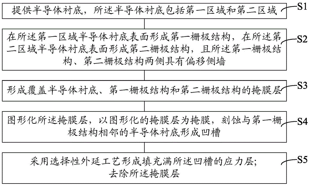
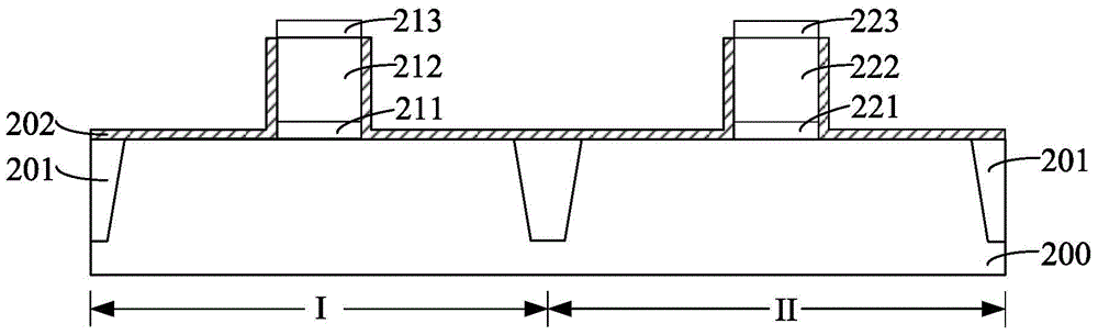
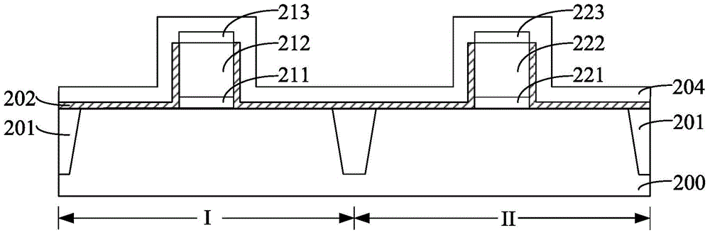
[0035] According to the research on the formation process of semiconductor devices, it is found that the formation process of semiconductor devices includes the following steps, please refer to figure 1: Step S1, providing a semiconductor substrate, the semiconductor substrate includes a first region and a second region; Step S2, forming a first gate structure on the surface of the semiconductor substrate in the first region, and forming a semiconductor substrate in the second region A second gate structure is formed on the surface of the substrate, and there are offset spacers on both sides of the first gate structure and the second gate structure; step S3, forming a covering semiconductor substrate, the first gate structure and the second gate structure A mask layer of the pole structure; step S4, patterning the mask layer, u...


PUM

PropertyMeasurementUnit
Thicknessaaaaaaaaaa

Abstract

A formation method of a semiconductor device comprises the steps of providing a substrate, wherein a grid structure is formed on the surface of the substrate; etching to remove the partial thickness of substrate at the two sides of the grid structure to form grooves; carrying out the oxidation treatment on the surfaces of the grooves to form oxidation films, and repairing the crystal lattice damage on the surfaces of the grooves; removing the oxidation films to expose the surfaces of the grooves; adopting an epitaxy process to form the stress layers filling the grooves. According to the present invention, before the stress layers are formed, the oxidation treatment is carried out on the surfaces of the grooves, the materials having the crystal lattice damage on the surfaces of the grooves are transformed into the oxidation film materials, and then the oxidation films are removed, so that the exposed crystal lattices on the surfaces of the grooves are high in quality, and accordingly, the stress layers of high quality and few defects are conducive to being formed, the stress actions of the stress layers in a channel region are larger, and a driving current of the formed semiconductor device is improved.

Description

technical field [0001] The invention relates to the technology in the field of semiconductor manufacturing, in particular to a method for forming a semiconductor device. Background technique [0002] With the continuous development of semiconductor technology, carrier mobility enhancement technology has been widely studied and applied. Improving the carrier mobility in the channel region can increase the driving current of MOS devices and improve the performance of the devices. [0003] In the existing manufacturing process of semiconductor devices, since stress can change the energy gap and carrier mobility of silicon materials, it has become more and more common means to improve the performance of semiconductor devices through stress. Specifically, by properly controlling the stress, the mobility of carriers (electrons in NMOS devices, holes in PMOS devices) can be increased, thereby increasing the driving current, thereby greatly improving the performance of semiconductor...

Claims


Application Information

Patent Timeline
IPC IPC(8): H01L21/20H01L21/8238
Inventor 丁士成沈忆华余云初
Owner SEMICON MFG INT (SHANGHAI) CORP
Why Eureka
Try Eureka