Manufacturing method for low temperature polycrystalline silicon thin film transistors

A technology of thin-film transistors and low-temperature polysilicon, which is applied in semiconductor/solid-state device manufacturing, electrical components, circuits, etc., can solve problems such as substrate unevenness, brightness deviation of display devices, substrate-to-substrate unevenness, etc., to improve uniformity and enhance The effect of improving productivity and uniformity

Inactive Publication Date: 2015-11-25
EVERDISPLAY OPTRONICS (SHANGHAI) CO LTD
View PDF3 Cites 6 Cited by
  • Summary
  • Abstract
  • Description
  • Claims
  • Application Information

AI Technical Summary

Problems solved by technology

If the above-mentioned electrical uniformity is poor, the driving current of the display device will be uneven, and as a result, problems such as brightness deviation and display unevenness of the display device will be caused.
This will not only cause unevenness within the same substrate (such as a 4.5-generation substrate with a size of 730mm×920mm), but also between substrates

Method used


Image

  • Manufacturing method for low temperature polycrystalline silicon thin film transistors
  • Manufacturing method for low temperature polycrystalline silicon thin film transistors
  • Manufacturing method for low temperature polycrystalline silicon thin film transistors

Examples


Embodiment

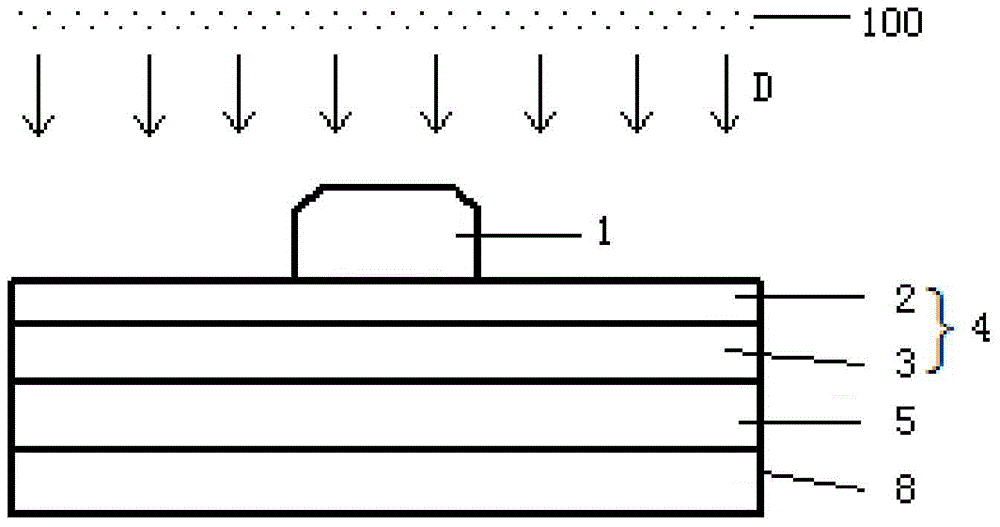
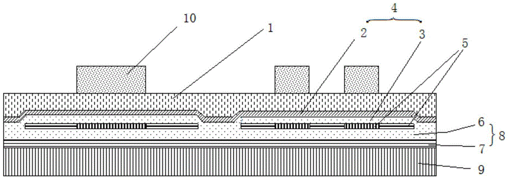
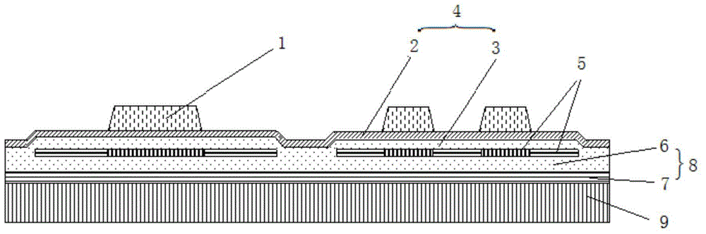
[0051] In the process of dry etching the gate metal, for example, dry etching equipment manufactured by Tokyo Electron Limited (TEL) can be used to implement etching using chlorine gas plasma, and only the metal molybdenum layer is etched to form the gate. Pole, and then demoulding and degumming. Here, the film thickness uniformity of the remaining first silicon nitride layer 2 was measured to be kept below 3% by using an ellipsometer.

[0052] In the process of penetrating the gate insulating layer, the dopant particles need to penetrate the first silicon nitride layer 2 and the first silicon dioxide layer 3 as the gate insulating layer 4 (respectively equivalent to figure 1 Silicon nitride layer 2 and silicon dioxide layer 3). Implement the lightly doped leakage implantation test, the dopant uses boron ions to incident dopant ions in the ion implantation direction D perpendicular to the substrate, and forms a lightly doped leakage implantation region in the polysilicon layer...


PUM


Abstract

The present invention provides a manufacturing method for low temperature polycrystalline silicon thin film transistors, and the method is characterized by including the following steps: a polycrystalline silicon layer, a gate insulation layer and a gate metal layer are formed on a substrate in sequence; one part of the gate metal layer is removed so as to expose one part of the gate insulating layer; and doping ions penetrate the exposed part of the gate insulation layer by the adoption of an ion-injection method. According to the invention, a metal layer is etched only but a silicon nitride and silicon oxide layer is not etched, a dose uniformity of the doping ion injecting is increased, and therefore, an electricity uniformity of the low temperature polycrystalline silicon thin film transistors is improved.

Description

technical field [0001] The invention relates to a method for manufacturing a low-temperature polysilicon thin film transistor, in particular to a method capable of improving the electrical uniformity of the low-temperature polysilicon thin film transistor. Background technique [0002] In the CMOS (ComplementaryMetalOxideSemiconductor: Complementary Metal Oxide Semiconductor) manufacturing process of low-temperature polysilicon thin film transistor (LTPSTFT), after the polysilicon gate structure process is implemented, that is, after the gate metal layer and gate insulating layer (GI: Gateinsulator) structure are formed, The ion implantation doping process is performed, that is, the "penetrating gate insulating layer process". [0003] For example, after forming the film structure of molybdenum (Mo) layer / silicon nitride (SiNx) layer / silicon oxide (SiO2) layer / polysilicon (Poly) layer / buffer (Buffer) layer, implement an ion implantation process, such as implementing light do...

Claims


Application Information

Patent Timeline
Patent Type & Authority Applications(China)
IPC IPC(8): H01L21/336
Inventor 严晓龙吴建宏彭思君钟尚骅
Owner EVERDISPLAY OPTRONICS (SHANGHAI) CO LTD
Why Eureka
Try Eureka