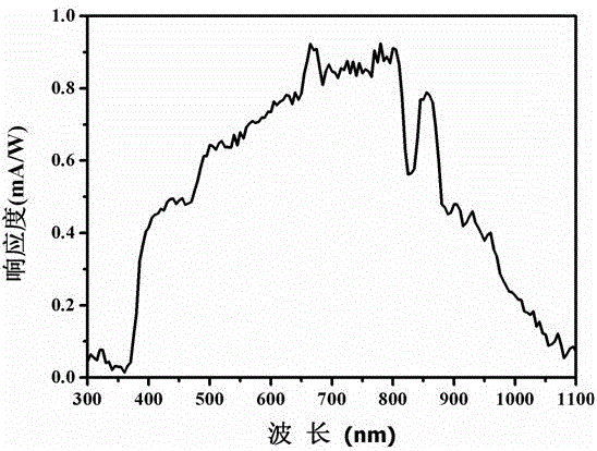
A heterojunction near-infrared photosensitive sensor and its preparation method
A near-infrared light, heterojunction technology, used in semiconductor devices, final product manufacturing, sustainable manufacturing/processing, etc., can solve problems such as not getting detectors
- Summary
- Abstract
- Description
- Claims
- Application Information
AI Technical Summary
Problems solved by technology
Method used
Image
Examples
preparation example Construction
[0021] The preparation and detection process of the heterojunction near-infrared photosensitive sensor of the present invention are as follows:
[0022] 1. Deposit a layer of Au with a thickness of 30-100 nm as a seed layer on a clean substrate by magnetron sputtering coating method.
[0023] 2. Put the evaporation source and the substrate into the controlled atmosphere tube furnace at the same time, and set the temperature of the evaporation source to 1000 o C, the substrate is placed at a distance of 7, 10, 13, 16 or 19 cm from the evaporation source, the heating rate is 10 ° C / min, and the temperature is kept for 10-30 min. The reaction atmosphere is Ar gas 20 sccm and O 2 8 sccm. The evaporation source is 0.255-0.265g ZnO powder, 0.040-0.060g carbon powder, 0.020-0.030g tellurium powder.
[0024] 3. After the reaction is completed, the substrate is taken out, and a solution of polymethyl methacrylate (PMMA) is spin-coated to fill the pores on the surface of the composi...
Embodiment 1
[0031] In this example, the substrate is placed on figure 1 In the 2 position. Specific steps are as follows:
[0032] 1. Clean the p-Si substrate by conventional semiconductor process.
[0033] 2. A 30nm Au thin film is deposited on the substrate as a seed layer.
[0034] 3. Put the substrate and evaporation source into a controlled atmosphere tube furnace, the substrate is 7 cm away from the evaporation source, and the temperature of the evaporation source is set to 1000 o C, heating rate 10°C / min, heat preservation 10min, the reaction atmosphere is Ar gas 20 sccm and O 2 8 sccm. The evaporation source is 0.261g ZnO powder, 0.043g carbon powder, 0.020g tellurium powder.
[0035] 4. After the reaction is completed, the substrate is taken out, and the PMMA solution is spin-coated to fill the pores on the surface of the composite.
[0036] 5. Continue to deposit a translucent metal Au top electrode by using a metal mask method.
[0037] 6. The InGa electrode is then doct...
Embodiment 2
[0042] In this example, the substrate is placed onfigure 1 In the 3 position. Specific steps are as follows:
[0043] 1. Clean the p-Si substrate by conventional semiconductor process.
[0044] 2. Deposit a 30 nm Au thin film on the substrate as a seed layer.
[0045] 3. Put the substrate and evaporation source into a controlled atmosphere tube furnace, the substrate is 10 cm away from the evaporation source, and the temperature of the evaporation source is set to 1000 o C, the heating rate is 10°C / min, the heat preservation is 30 min, and the reaction atmosphere is Ar gas 20 sccm and O 2 8 sccm. The evaporation source is 0.264g ZnO powder, 0.053g carbon powder, 0.024g tellurium powder.
[0046] 4. After the reaction is completed, the substrate is taken out, and the PMMA solution is spin-coated to fill the pores on the surface of the composite.
[0047] 5. Continue to deposit a translucent metal Au top electrode by using a metal mask method.
[0048] 6. The InGa electrod...
PUM
 Abstract
Description
Claims
Application Information


