Heterojunction near-infrared photosensitive sensor and preparation method thereof

A near-infrared light, heterojunction technology, used in semiconductor devices, final product manufacturing, sustainable manufacturing/processing, etc., can solve problems such as lack of detectors

Active Publication Date: 2015-11-25
WUHAN UNIV
View PDF3 Cites 4 Cited by
  • Summary
  • Abstract
  • Description
  • Claims
  • Application Information

AI Technical Summary

Problems solved by technology

However, since zinc oxide is sensitive to ultraviolet light and silicon is sensitive to visible-near-infrared light, the heterojunction photosensitive detectors formed by the two are also limited by this, and no purer detectors that are only sensitive to near-infrared light have been obtained. device

Method used


Image

  • Heterojunction near-infrared photosensitive sensor and preparation method thereof
  • Heterojunction near-infrared photosensitive sensor and preparation method thereof
  • Heterojunction near-infrared photosensitive sensor and preparation method thereof

Examples


preparation example Construction

[0021] The preparation and detection process of the heterojunction near-infrared photosensitive sensor of the present invention are as follows:

[0022] 1. Deposit a layer of Au with a thickness of 30-100 nm as a seed layer on a clean substrate by magnetron sputtering coating method.

[0023] 2. Put the evaporation source and the substrate into the controlled atmosphere tube furnace at the same time, and set the temperature of the evaporation source to 1000 o C, the substrate is placed at a distance of 7, 10, 13, 16 or 19 cm from the evaporation source, the heating rate is 10 ° C / min, and the temperature is kept for 10-30 min. The reaction atmosphere is Ar gas 20 sccm and O 2 8 sccm. The evaporation source is 0.255-0.265g ZnO powder, 0.040-0.060g carbon powder, 0.020-0.030g tellurium powder.

[0024] 3. After the reaction is completed, the substrate is taken out, and a solution of polymethyl methacrylate (PMMA) is spin-coated to fill the pores on the surface of the composi...

Embodiment 1

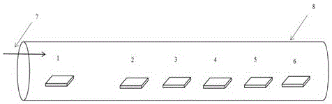
[0031] In this example, the substrate is placed on figure 1 In the 2 position. Specific steps are as follows:

[0032] 1. Clean the p-Si substrate by conventional semiconductor process.

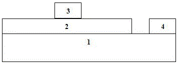
[0033] 2. A 30nm Au thin film is deposited on the substrate as a seed layer.

[0034] 3. Put the substrate and evaporation source into a controlled atmosphere tube furnace, the substrate is 7cm away from the evaporation source, and the temperature of the evaporation source is set to 1000 o C, heating rate 10°C / min, heat preservation 10min, the reaction atmosphere is Ar gas 20sccm and O 2 8 sccm. The evaporation source is 0.261g ZnO powder, 0.043g carbon powder, 0.020g tellurium powder.

[0035] 4. After the reaction is completed, the substrate is taken out, and the PMMA solution is spin-coated to fill the pores on the surface of the composite.

[0036] 5. Continue to deposit a translucent metal Au top electrode by using a metal mask method.

[0037] 6. The InGa electrode is then doctor...

Embodiment 2

[0042] In this example, the substrate is placed on figure 1 In the 3 position. Specific steps are as follows:

[0043] 1. Clean the p-Si substrate by conventional semiconductor process.

[0044] 2. A 30nm Au thin film is deposited on the substrate as a seed layer.

[0045]3. Put the substrate and evaporation source into a controlled atmosphere tube furnace, the substrate is 10cm away from the evaporation source, and the temperature of the evaporation source is set to 1000 o C, heating rate 10°C / min, heat preservation 30min, the reaction atmosphere is Ar gas 20sccm and O 2 8 sccm. The evaporation source is 0.264g ZnO powder, 0.053g carbon powder, 0.024g tellurium powder.

[0046] 4. After the reaction is completed, the substrate is taken out, and the PMMA solution is spin-coated to fill the pores on the surface of the composite.

[0047] 5. Continue to deposit a translucent metal Au top electrode by using a metal mask method.

[0048] 6. The InGa electrode is then doctor...


PUM


Abstract

The invention belongs to the field of photoelectrons, and relates to a heterojunction near-infrared photosensitive sensor and a preparation method thereof. The heterojunction near-infrared photosensitive sensor is a heterojunction photosensitive sensor which is formed by a zinc tellurium oxide compound and p-Si, wherein the zinc tellurium oxide compound is prepared by a thermal evaporation vapor deposition method; and the heterojunction near-infrared photosensitive sensor comprises a p-type silicon substrate, the zinc tellurium oxide compound, a top electrode and a bottom electrode. The key of the heterojunction near-infrared photosensitive sensor is preparation of the zinc tellurium oxide compound. The novel sensor shows stable and excellent photosensitive detection performance of an adjustable waveband; and the near-infrared waveband of which the wavelength is adjusted to 1040nm from an ultraviolet-visible-near-infrared waveband can be detected.

Description

technical field [0001] The invention belongs to the field of preparation and application of nanometer materials, and also belongs to the field of optoelectronics, and relates to a silicon / telluride-zinc-oxygen compound heterojunction near-infrared photosensitive sensor and a preparation method thereof. Background technique [0002] Silicon material is the cornerstone of the contemporary semiconductor industry and has extremely important applications in the field of photosensitive detection. The spectral response range of traditional Si detectors is generally 400-1100nm. In recent years, Si and some other semiconductor materials such as graphene (ZhuM, ZhangL, LiX, HeY, LiX, GuoF, ZhangX, WangK, XieD, LiX, WeiBandZhuH2015J.Mater.Chem.A78133), zinc oxide (TsaiDH, LinCA, LienWC, ChangHC, WangYLandHeJH2011ACSNano57748), copper oxide (HongQ, CaoY, XuJ, LuH, HeJandSunJL2014ACSAppl.Mater.Interfaces620887), PEDOT:PSS (LinT, LiuX, ZhouB, ZhanZ, CartwrightANandSwihartMT2014AdvMan2Func...

Claims


Application Information

Patent Timeline
Patent Type & Authority Applications(China)
IPC IPC(8): H01L31/109H01L31/0296H01L31/18
CPCH01L31/02966H01L31/109H01L31/1832Y02P70/50
Inventor 方国家宋增才李博睿
Owner WUHAN UNIV
Why Eureka
Try Eureka