Making method for transmission array of field radiation cathode carbon nano pipe

A field emission cathode and carbon nanotube technology, which is applied in cold cathode manufacturing, discharge tube/lamp manufacturing, electrode system manufacturing, etc., to achieve the effects of simple process, cost saving and low cost

Inactive Publication Date: 2008-08-06
WUHAN UNIV
View PDF0 Cites 7 Cited by
  • Summary
  • Abstract
  • Description
  • Claims
  • Application Information

AI Technical Summary

Problems solved by technology

Formation of carbon nanotube emission arrays after electric field annealing and aging treatment

Method used


Image

  • Making method for transmission array of field radiation cathode carbon nano pipe
  • Making method for transmission array of field radiation cathode carbon nano pipe

Examples


Embodiment 1

[0023] Embodiment 1: In this embodiment, a silicon wafer is used as a substrate and a metal mask is used as an example for illustration. Specific steps are as follows:

[0024] 1. Use semiconductor standard cleaning technology for silicon wafers (such as: Yan Zhirui, Development Direction of Semiconductor Silicon Wafer Cleaning Technology, Special Equipment for Electronic Industry, 2003, September, p23-26), to clean single-sided polished silicon wafers.

[0025] 2. Attach a metal mask with holes and regularly arranged on a clean silicon wafer, and use magnetron sputtering to coat a metal Sn film with a thickness of about 50 nanometers. A Ni catalyst layer is then plated on it, with a thickness of about 20 nanometers. A Ni / Sn binary composite catalyst array layer is formed.

[0026] 3. The substrate is plated with the Ni / Sn binary composite catalyst array facing down, facing the middle of the burning ethanol (analytical pure) flame for 1-30 minutes, and growing carbon nanotub...

Embodiment 2

[0029] Embodiment 2: In this embodiment, a metal molybdenum sheet is used as a substrate, and conventional photolithography technology is used as an example for illustration. Specific steps are as follows:

[0030] 1. Use deionized water, acetone and absolute ethanol to repeatedly ultrasonically clean the molybdenum sheet.

[0031] 2. Traditional semiconductor photolithography technology uses magnetron sputtering to coat metal Zn film with a thickness of about 50 nanometers, and makes indium tin alloy lattice on molybdenum sheet. A Fe-Ni composite catalyst layer is plated on it by a sputtering coating process, and the catalyst layer has a thickness of about 20 nanometers. A FeNi / Zn composite catalyst array layer is formed.

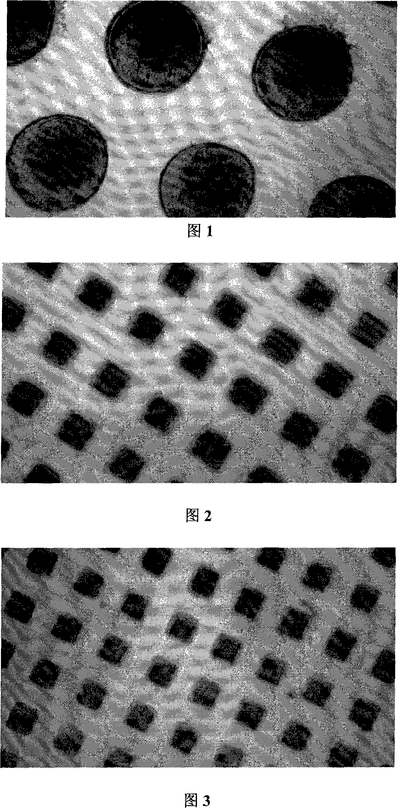
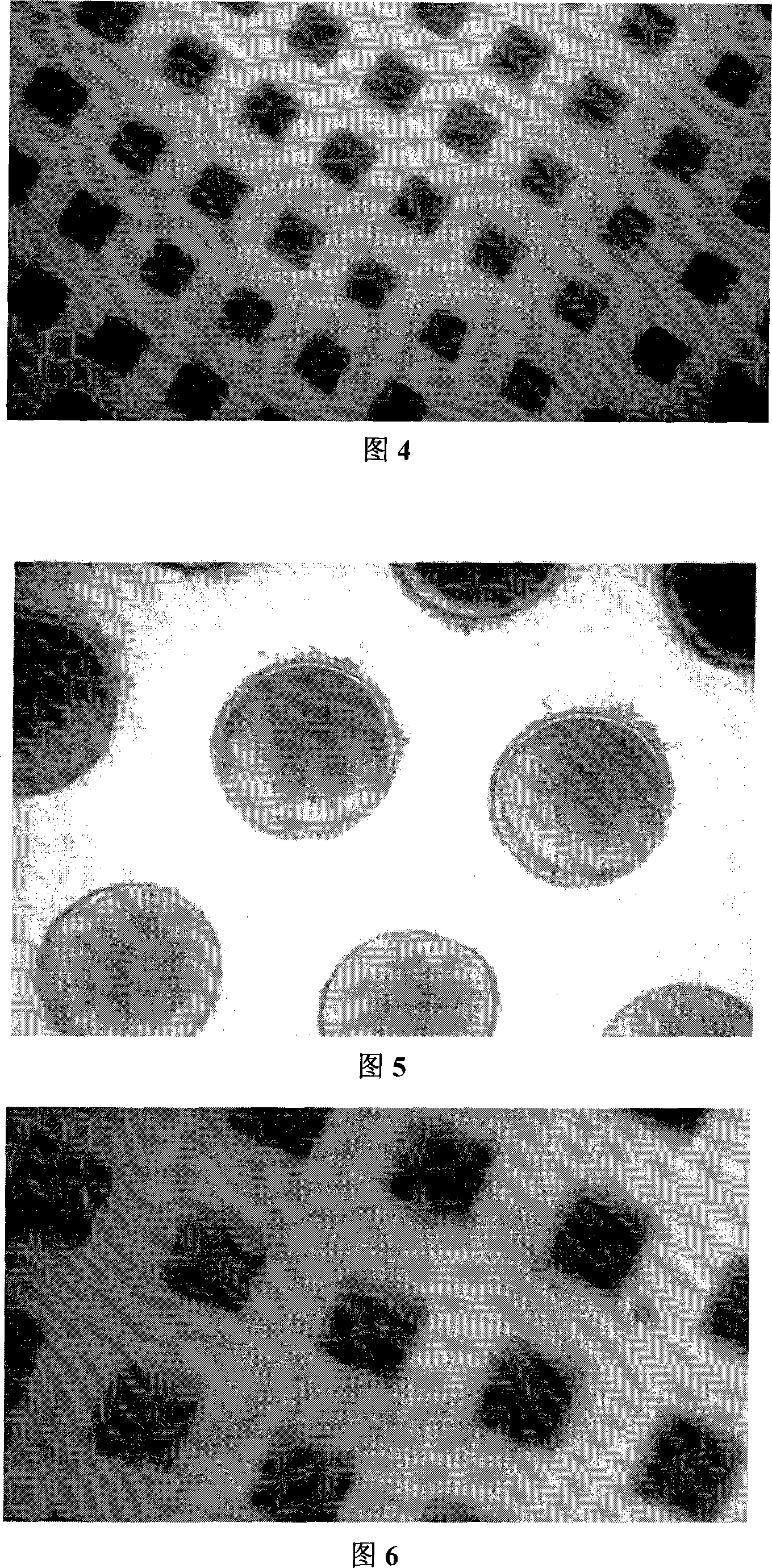
[0032] 3. Put the substrate plated with the FeNi / Zn composite catalyst array face down, facing the middle of the burning acetylene flame for 1-30 minutes, and grow carbon nanotubes on the catalyst. Fig. 2 is an optical microscope photo of a carbon nanot...

Embodiment 3

[0035] Embodiment 3: In this embodiment, a metal tantalum sheet is used as a substrate and conventional photolithography technology is used as an example for illustration. Specific steps are as follows:

[0036] 1. Use deionized water, acetone and absolute ethanol to repeatedly ultrasonically clean the tantalum sheet.

[0037] 2. Traditional semiconductor photolithography technology uses sputtering coating technology to make indium-tin alloy lattices on tantalum wafers, with a thickness of about 10 nanometers, and then plate a Ni catalyst layer on them, with a thickness of about 10 nanometers. A Ni / InSn composite catalyst array layer is formed.

[0038] 3. The substrate plated with the Ni / InSn composite catalyst array faces downward, facing the middle of the burning ethylene propanol flame for 1-30 minutes, and growing carbon nanotubes on the catalyst. Fig. 3 is an optical microscope photo of a carbon nanotube array.

[0039] 4. The tantalum sheet with nanotubes is placed o...


PUM

PropertyMeasurementUnit
thicknessaaaaaaaaaa

Abstract

The invention relates to a method for preparing a carbon nano-tube array field emission cathode, including the following steps that: the mask is made by a metal mask plate or the photoresist; a low melting point metal layer is deposited on a substrate, and a catalyst layer is deposited on the low melting point metal layer, forming a lower melting point metal-catalyst composite lattice; and then the lower melting point metal-catalyst composite lattice is burnt in a flame for 1 to 10 minutes, and the stable carbon nano-tube emission array is formed after the annealing and ageing treatment of the electric field. The method for preparing a carbon nano-tube array field emission cathode has the advantages of easy operation, low cost and unnecessary nitride or oxide transition layer; moreover, the invention can grow the carbon nano-tube array under an open atmospheric environment(vacuum equipments are not needed) and finish the preparation of the growth of the carbon nano-tube and the assembly of the cold cathode array at one time; moreover, the prepared carbon nano-tube array has the advantages of large area, even and localized growth and desirable emission characteristics. The carbon nano-tube array prepared by the invention can be used as the emission cathode to be applied to a field emission displayer or a luminous light source, an X-ray electron source, a mass spectrograph electron source and other occasions where the electron source is needed.

Description

technical field [0001] The invention relates to a method for preparing a carbon nanotube array field emission cathode, in particular to a method for preparing a carbon nanotube array cold cathode through a flame combustion process, which belongs to the field of nanomaterial preparation and application, and also belongs to the field of vacuum microelectronics. Background technique [0002] As a one-dimensional nanomaterial, carbon nanotubes (CNTs) are light in weight, perfectly connected in a hexagonal structure, have many abnormal mechanical, electrical and chemical properties, and also have a high aspect ratio, extremely small tip radius, and high With mechanical strength and high current carrying capacity, it can be used as an excellent field emission source, and has important application prospects in the fields of vacuum electronics such as flat-panel displays, X-ray sources, microwave amplifiers, and lighting fixtures. Carbon nanotubes are expected to become one of the p...

Claims


Application Information

Patent Timeline
Patent Type & Authority Applications(China)
IPC IPC(8): H01J9/02
Inventor 方国家刘逆霜杨晓霞李春李军
Owner WUHAN UNIV
Why Eureka
Try Eureka