
Vertical interconnection structure for three-dimensional package based on aluminum substrates and preparation method thereof

A technology of vertical interconnection and three-dimensional packaging, which is applied in semiconductor/solid-state device manufacturing, electrical components, electrical solid-state devices, etc. It can solve the performance requirements of flexible substrates that cannot meet high-temperature service, thermal-mechanical damage of devices, residual stress of solder joints, etc. problem, achieve the effect of improving packaging efficiency and interconnection density, reducing manufacturing cost, and good strength

Active Publication Date: 2015-12-02
SHANGHAI SPACEFLIGHT ELECTRONICS & COMM EQUIP RES INST
View PDF4 Cites 8 Cited by
  • Summary
  • Abstract
  • Description
  • Claims
  • Application Information

AI Technical Summary

Problems solved by technology

Due to the parasitic resistance and distributed inductance of the lead wires, the obvious electromagnetic coupling phenomenon in high-frequency applications will cause thermo-mechanical damage, signal mutual interference, and signal loss to the device; The performance difference of some intermetallic compounds limits its application in the field of high-density packaging, and at the same time, the solder bump interconnection will lead to the existence of residual stress inside the solder joint due to its high process temperature and low rheological rate; flexible substrate Can not meet the performance requirements of high temperature service

Method used


Image

  • Vertical interconnection structure for three-dimensional package based on aluminum substrates and preparation method thereof
  • Vertical interconnection structure for three-dimensional package based on aluminum substrates and preparation method thereof
  • Vertical interconnection structure for three-dimensional package based on aluminum substrates and preparation method thereof

Examples


Embodiment 1

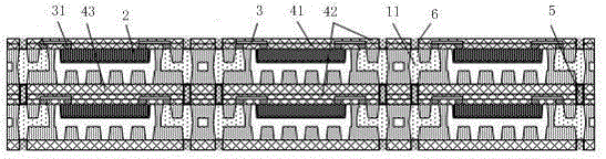
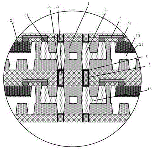
[0073] to combine Figure 1-Figure 2 , this embodiment describes in detail the aluminum substrate-based three-dimensional packaging vertical interconnection structure of the present invention, which includes: functionalized aluminum substrate 1, embedded chip 2, thin film interconnection 3, dielectric layer 4 and intermetallic compound interconnection Line 5, functionalized aluminum plate 1 includes: aluminum through post 11, aluminum half-through post 12, grounding aluminum post 13, chip embedding cavity 14, buried aluminum ground layer 15 and buried aluminum interconnection line 16, chip embedding cavity 14 is set On the upper surface of the functionalized aluminum substrate, it is a concave structure; one side of the embedded aluminum ground layer 15 is connected to the lower end of the chip embedding cavity 14, and the other side is connected to the grounded aluminum column 13; the aluminum through column 11 penetrates the upper and lower sides of the functionalized aluminu...

Embodiment 2

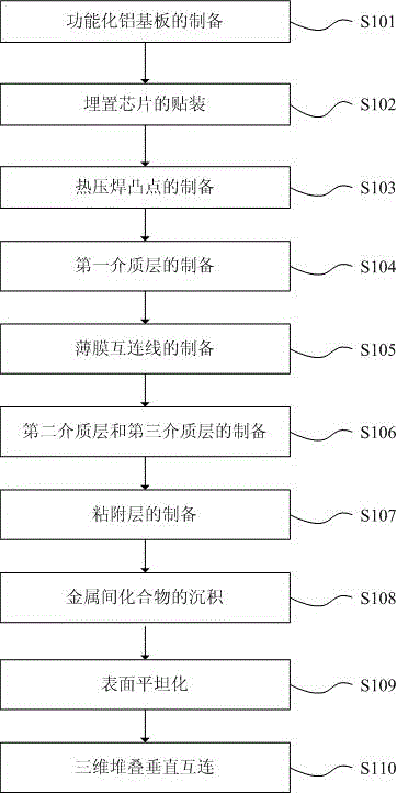
[0079] to combine image 3 - Fig. 4, this embodiment describes in detail the preparation method of the vertical interconnection structure for three-dimensional packaging based on the aluminum substrate of the present invention, which includes the following steps:

[0080] S101: Preparation of functionalized aluminum substrates: provide a pair of polished aluminum substrates, and prepare functionalized aluminum substrates through multiple photolithography and multiple anodic oxidations. The formed functionalized aluminum substrates include: aluminum through pillars 11, aluminum half through pillars 12, Grounding aluminum post 13, buried aluminum ground layer 15 and buried aluminum interconnection 16, aluminum through post 11 penetrates the upper and lower surfaces of functionalized aluminum substrate 1, aluminum half-through post 12 penetrates the upper surface of functionalized aluminum substrate 1, buried aluminum interconnection The connection line 16 is connected to the alu...

Embodiment 3

[0095] The difference between this embodiment and Embodiment 2 is that the thin film interconnection lines are formed in different ways. like Figure 5a , 5b As shown, the thin-film interconnection lines used to connect the embedded chip 2 and the aluminum half-through pillar 12 are directly interconnected through the dielectric hole 411 formed on the first dielectric layer 41 by photolithography and development.


PUM

PropertyMeasurementUnit
Melting pointaaaaaaaaaa
Thicknessaaaaaaaaaa
Single layer thicknessaaaaaaaaaa

Abstract

The present invention discloses a vertical interconnection structure for three-dimensional package based on aluminum substrates and a preparation method thereof. The structure comprises at least two layers of functionalized aluminum substrates. Each of the aluminum substrates comprises an aluminum through column, an aluminum semi-through column, a grounded aluminum column, a chip embedded cavity, an aluminum buried grounded layer and an aluminum embedded interconnection line. The vertical interconnection structure comprises embedded chips which are embedded in the chip embedded cavities of the functionalized aluminum substrates, film interconnection lines whose two ends are connected to the embedded chips and the aluminum through columns, intermetallic compound vertical interconnect lines whose two ends are connected to the aluminum through columns of two adjacent layers of functionalized aluminum substrates, and dielectric layers which are arranged at the surfaces of the functionalized aluminum substrates. The method comprises the preparation of the functionalized aluminum plate, the surface mounting of the embedded chips, the preparation of the film interconnection lines, the preparation of the dielectric layers, the deposition of the intermetallic compound, and the 3D stacked vertical interconnection. According to the vertical interconnection structure and the preparation method, the package efficiency and interconnection density are raised, and the intermetallic compound vertical interconnection is used to achieve the effect of 'low temperature preparation and high temperature use'.

Description

technical field [0001] The invention relates to the field of microelectronic packaging, in particular to a vertical interconnection structure for three-dimensional packaging based on an aluminum substrate and a preparation method thereof. Background technique [0002] Driven by "Following Moore's Law" and "Beyond Moore's Law", microelectronic packaging is developing towards high integration density, high power density, high reliability and low cost. During the development of packaging form from single-chip packaging to three-dimensional packaging, higher requirements are put forward for the structural stress matching and high-temperature service performance of the packaging. The interconnection technology that can meet the requirements of high interconnection density, high power density, and low-temperature bonding for future three-dimensional packaging is attracting the attention of academia and industry. [0003] Three-dimensional integration technology is the key technol...

Claims


Application Information

Patent Timeline
IPC IPC(8): H01L23/48H01L23/31H01L21/60
CPCH01L2224/18H01L2224/32245H01L2224/73267H01L2224/92244H01L2924/15153H01L23/48
Inventor 吴伟伟赵涌刘米丰谢慧琴丁蕾王立春
Owner SHANGHAI SPACEFLIGHT ELECTRONICS & COMM EQUIP RES INST
Learn More