Sapphire substrate-based multilayer gallium oxide thin film and growing method thereof
A technology of a sapphire substrate and a growth method, applied in the field of microelectronics, can solve the problems of poor surface morphology and small grain size of Ga2O3 thin films, and achieve the effects of improving surface morphology, increasing seed crystal nucleation density, and improving coverage.
- Summary
- Abstract
- Description
- Claims
- Application Information
AI Technical Summary
Problems solved by technology
Method used
Image

Examples
Embodiment 1
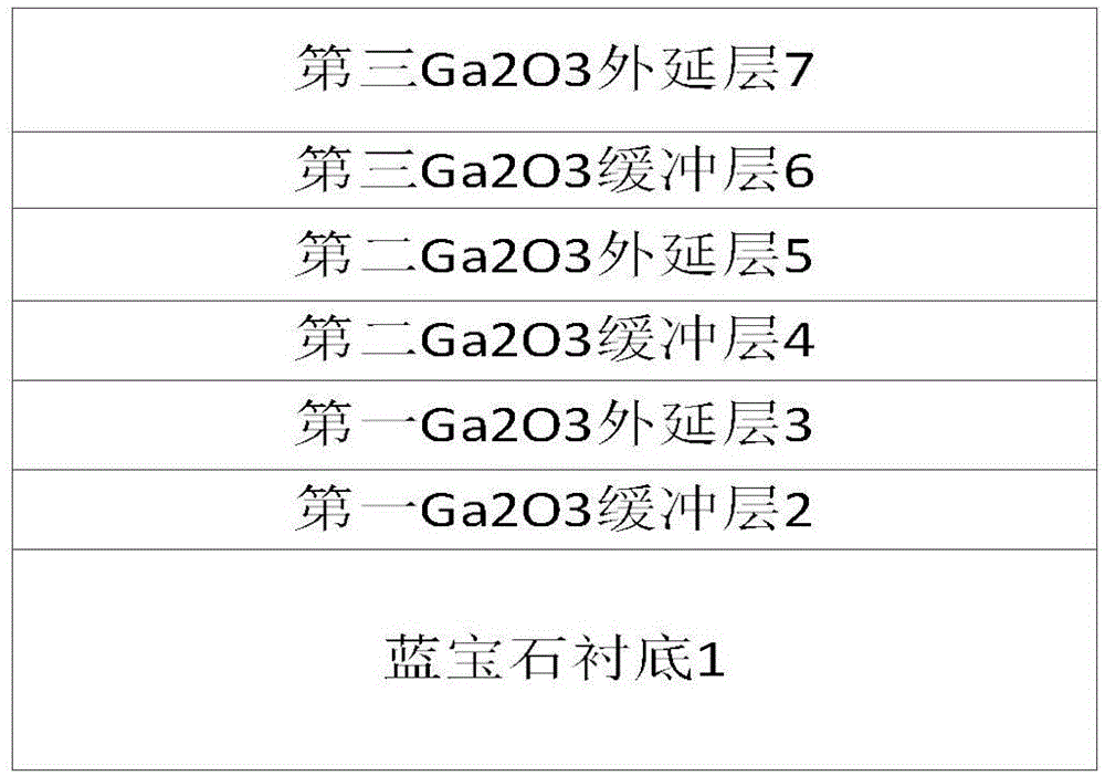
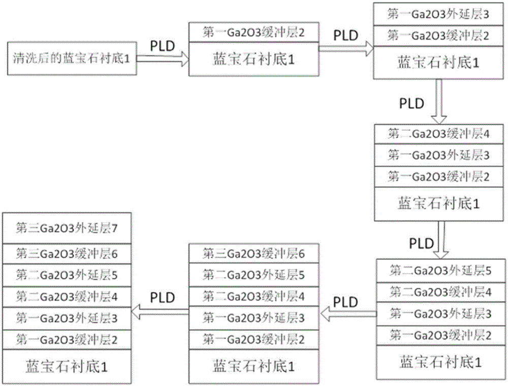
[0023] Example 1, a multilayer gallium oxide thin film containing three composite layers is fabricated on a sapphire substrate.
[0024] refer to figure 1 , the multilayer gallium oxide thin film of this embodiment comprises a sapphire substrate 1, a first gallium oxide buffer layer 2, a first gallium oxide epitaxial layer 3, a second gallium oxide buffer layer 4, a second gallium oxide epitaxial layer from bottom to top 5. The third gallium oxide buffer layer 6 and the third gallium oxide epitaxial layer 7 . Wherein the substrate 1 is a sapphire substrate with (0001) orientation, the third gallium oxide epitaxial layer 7 adopts Ga2O3 material with a thickness of 25nm, the first gallium oxide buffer layer 2, the second gallium oxide buffer layer 4 and the third gallium oxide buffer layer Layer 6 is made of Ga2O3 material with a thickness of 8nm, the first gallium oxide epitaxial layer 3 is made of Ga2O3 material with a thickness of 15nm, and the second gallium oxide epitaxial...
Embodiment 2
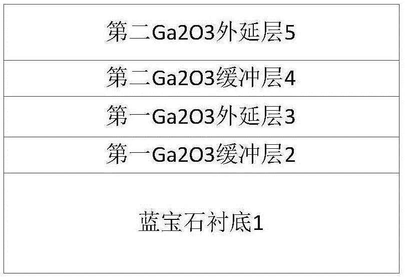
[0047] Example 2, a multilayer gallium oxide thin film containing two composite layers is fabricated on a sapphire substrate.
[0048] refer to image 3 , the multilayer gallium oxide thin film of this embodiment comprises a sapphire substrate 1, a first gallium oxide buffer layer 2, a first gallium oxide epitaxial layer 3, a second gallium oxide buffer layer 4 and a second gallium oxide epitaxial layer from bottom to top 5. Wherein the substrate 1 is a sapphire substrate of (0001) orientation, the first gallium oxide buffer layer 2 and the second gallium oxide buffer layer 4 adopt Ga2O3 material with a thickness of 12nm, the first gallium oxide buffer layer 2 and the first gallium oxide buffer layer The epitaxial layer 3 forms the first composite layer; as described; the first gallium oxide epitaxial layer 3 adopts a Ga2O3 material with a thickness of 20nm, and the second gallium oxide epitaxial layer 5 adopts a Ga2O3 material with a thickness of 25nm. The second gallium oxi...
Embodiment 3
[0070] Example 3, a gallium oxide thin film containing four composite layers is fabricated on a sapphire substrate.
[0071] refer to Figure 5 , the multilayer gallium oxide thin film of this embodiment comprises a sapphire substrate 1, a first gallium oxide buffer layer 2, a first gallium oxide epitaxial layer 3, a second gallium oxide buffer layer 4, a second gallium oxide epitaxial layer from bottom to top 5. The third gallium oxide buffer layer 6 , the third gallium oxide epitaxial layer 7 , the fourth gallium oxide buffer layer 8 and the fourth gallium oxide epitaxial layer 9 . Wherein the substrate 1 is a sapphire substrate with (0001) orientation, the fourth gallium oxide epitaxial layer 9 adopts Ga2O3 material with a thickness of 25nm, the first gallium oxide buffer layer 2, the second gallium oxide buffer layer 4, the third gallium oxide buffer layer Layer 6 and the fourth gallium oxide buffer layer 8 adopt Ga2O3 material with a thickness of 10nm, the first gallium ...
PUM
| Property | Measurement | Unit |
|---|---|---|
| thickness | aaaaa | aaaaa |
| thickness | aaaaa | aaaaa |
| thickness | aaaaa | aaaaa |
Abstract
Description
Claims
Application Information
 - R&D
- Intellectual Property
- Life Sciences
- Materials
- Tech Scout
- Unparalleled Data Quality
- Higher Quality Content
- 60% Fewer Hallucinations
Browse by: Latest US Patents, China's latest patents, Technical Efficacy Thesaurus, Application Domain, Technology Topic, Popular Technical Reports.
© 2025 PatSnap. All rights reserved.Legal|Privacy policy|Modern Slavery Act Transparency Statement|Sitemap|About US| Contact US: help@patsnap.com