
Infrared blocking filter, solid-state imaging device, imaging device, and display device

A technology for shielding filters and infrared rays, applied in the direction of electric solid devices, electrical components, optical components, etc., can solve the problems of reduced product yield, increased number of resulting processes, and increased number of layers, etc., to achieve the effect of high transmittance

Active Publication Date: 2017-07-21
ASAHI GLASS CO LTD
View PDF5 Cites 0 Cited by
  • Summary
  • Abstract
  • Description
  • Claims
  • Application Information

AI Technical Summary

Problems solved by technology

However, in this case, the thickness of the device cannot be met, such as the above-mentioned thinning requirements of the digital camera.
In addition, it is also possible to extend the shielded wavelength region caused by the dielectric multilayer film to a long wavelength region exceeding 1200 nm, but the number of laminations and the total film thickness must be increased, resulting in an increase in the number of steps, and there is also a problem of adhesion to the film during film formation. The problem of foreign matter on the surface, the reduction of product yield, the increase of manufacturing cost and other issues

Method used


Image

  • Infrared blocking filter, solid-state imaging device, imaging device, and display device
  • Infrared blocking filter, solid-state imaging device, imaging device, and display device
  • Infrared blocking filter, solid-state imaging device, imaging device, and display device

Examples


Embodiment 1

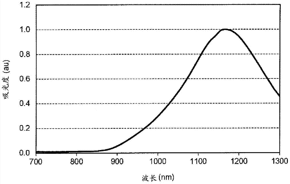
[0198] In a 15% by mass cyclohexanone solution of polyester resin (trade name B-OKP2 manufactured by Osaka Gas Chemicals Co., Ltd.), the dithiolane complex represented by the formula (F1-6) (dissolved in toluene and measured In the absorption spectrum of light in the wavelength region of 700-1300nm, λ max for 1168nm, the λ maxThe absorbance is 1, and the absorbance is 0.2, and the shortest wavelength is 891nm) Mixed at a ratio of 4.0 parts by mass of the disulfide complex to 100 parts by mass of the polyester resin, stirred well to dissolve, and prepared coating solution A .

[0199] In a 50% by mass tetrahydrofuran solution of an acrylic resin (trade name OGSOLEA-F5003 manufactured by Osaka Gas Chemicals Co., Ltd.), a squarylium dye (λmax=697 nm (toluene)) represented by the following formula was added in an amount of 100% by mass to the acrylic resin. 0.25 parts by mass of squarylium pigment was mixed, fully stirred to dissolve, and coating solution B was prepared.

[020...

Embodiment 2

[0206] Coating liquid A and coating liquid B were prepared similarly to Example 1.

[0207] The coating solution A was applied to one main surface of the glass substrate by a die coating method, and after drying at room temperature for 5 minutes under reduced pressure (about 670 Pa), it was heated at 90° C. for 30 minutes. After repeating the steps from coating to heating again, heating was performed at 150° C. for 15 minutes to form an infrared absorbing layer A having a thickness of 10.8 μm. As the glass substrate, a substrate made of soda glass (manufactured by SCHOTT, trade name D263) having a thickness of 1.0 mm was used.

[0208] Next, on the above-mentioned infrared absorbing layer A, silicon dioxide (SiO 2 ; Refractive index 1.45 (wavelength 550nm)) layer and titanium dioxide (TiO 2 ; Refractive index 2.32 (wavelength 550nm)) layer, form the dielectric multilayer film A (42 layers) that is formed by the composition shown in Table 1.

[0209] Next, the coating liquid...

Embodiment 3

[0212] In the absorption spectrum measured using the disulfide compound (dissolved in toluene) shown in formula (F1-7), λ max for 1170nm, the λ max The absorbance is 1, and the absorbance is 0.2, and the shortest wavelength is 966 nm) instead of the disulfide compound shown in the formula (F1-6), the coating solution A is prepared in the same manner as in Example 1. cloth liquid.

[0213] This coating solution was applied to one main surface of a glass substrate by a die coating method, dried at room temperature for 5 minutes under reduced pressure (about 670 Pa), and then heated at 90° C. for 30 minutes. After repeating the steps from this application to heating again, it was heated at 150° C. for 15 minutes to form an infrared absorbing layer with a thickness of 4.7 μm. As the glass substrate, a substrate made of CuO-containing fluorophosphate glass (manufactured by AGC Techno Glass Co., Ltd., trade name NF-50T) having a thickness of 0.35 mm was used.

[0214] Next, silic...


PUM

PropertyMeasurementUnit
full width at half maximumaaaaaaaaaa
glass transition temperatureaaaaaaaaaa
thicknessaaaaaaaaaa

Abstract

An infrared shielding filter provided with an infrared absorbing layer made of a transparent resin containing an infrared absorber and a selective wavelength shielding layer laminated on the infrared absorbing layer, satisfying the following conditions: (i) spectral transmission at an incident angle of 0 degrees In the rate curve, the average transmittance at a wavelength of 450 to 600 nm is more than 80%, and the transmittance at a wavelength of 700 to 1200 nm is less than 2.0%. The change in transmittance D0 expressed by the following formula is less than 0.04, D0 (% / nm) = (Tmax·0‑Tmin·0) / (λ(Tmax·0)‑λ(Tmin·0)) (ii) In the spectral transmittance curve at an incident angle of 30 degrees, the average transmittance at wavelengths of 450 to 600 nm is 80 % or more, the transmittance at a wavelength of 700 to 1200 nm is less than 2.0%, the change in transmittance D30 expressed by the following formula is less than 0.04, D30 (% / nm) = (Tmax·30-Tmin·30) / (λ(Tmax· 30)-λ(Tmin·30)).

Description

technical field [0001] The present invention relates to an infrared shielding filter, a solid-state imaging device and an imaging / display device using the infrared shielding filter. Background technique [0002] In recent years, infrared shielding filters that transmit light in the visible wavelength range (420 to 630 nm) and block light in the near infrared wavelength range (700 to 1100 nm) have been used in various applications. [0003] For example, digital cameras, digital video, mobile phone cameras, etc. that use solid-state imaging elements such as CCD (Charge Coupled Device), CMOS image sensor (Complementary Metal Oxide Semiconductor Image Sensor, Complementary Metal Oxide Semiconductor ImageSensor), etc. Devices and display devices such as automatic illuminometers using light receiving elements have conventionally had spectral sensitivities ranging from the visible light wavelength region to the near-infrared wavelength region near 1100 nm. Therefore, in order to m...

Claims


Application Information

Patent Timeline
Patent Type & Authority Patents(China)
IPC IPC(8): G02B5/28C09B57/10C09K3/00G02B5/22H01L27/14H04N5/238H04N9/07H04N23/12H04N23/75
CPCC09B57/10G02B5/223C09B49/12G02B5/208G03B11/00
Inventor 山本今日子村上贵章馆村满幸熊井裕
Owner ASAHI GLASS CO LTD
Learn More