Multi-layer circuit board riveting structure, and suspended line circuit constituted by same, and realization method for suspended line circuit

A multi-layer circuit board and riveting structure technology, which is applied in multi-layer circuit manufacturing, printed circuit, printed circuit manufacturing, etc., can solve the problems of processing machinery cavity and high cost of multi-layer board circuit lamination process, and achieve small size, The effect of light weight and low cost

Active Publication Date: 2015-12-09
UNIV OF ELECTRONICS SCI & TECH OF CHINA
View PDF5 Cites 6 Cited by
  • Summary
  • Abstract
  • Description
  • Claims
  • Application Information

AI Technical Summary

Problems solved by technology

[0005] The purpose of the present invention is to provide a multilayer circuit board riveting structure and the suspension line circuit and its implementation method, which can realize the riveting processing of the multilayer circuit board and the riveting processing of the new medium integrated suspension line circuit, and solve the existing problems Laminate circuit lamination process costs are high, and traditional waveguide suspension line circuits need to process mechanical cavities and additional manual assembly, etc.

Method used


Image

  • Multi-layer circuit board riveting structure, and suspended line circuit constituted by same, and realization method for suspended line circuit
  • Multi-layer circuit board riveting structure, and suspended line circuit constituted by same, and realization method for suspended line circuit
  • Multi-layer circuit board riveting structure, and suspended line circuit constituted by same, and realization method for suspended line circuit

Examples


specific Embodiment

[0033] Example 1:

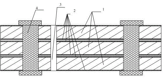
[0034] Multilayer circuit board riveting structure, including at least 2 layers of laminated circuit boards. The circuit board includes a dielectric substrate and metal layers arranged on the front and back of the dielectric substrate. After the circuit boards are laminated to form a multilayer circuit board body, in the multilayer circuit The board body is provided with a rivet hole, and a rivet is inserted into the rivet hole, the upper end of the rivet is crimped with the upper surface of the multilayer circuit board body, and the lower end of the rivet is crimped with the lower surface of the multilayer circuit board body. Rivet holes can be metallized or non-metallized.

[0035] From the above structure, we can see that there is a zero-gap contact between adjacent circuit boards, so the present invention does not require traditional bonding material layers (such as prepregs) between adjacent circuit boards. The present invention can use the commonly u...

Embodiment approach 1

[0039] Embodiment 1: For ordinary multilayer circuit board riveting, when the number of circuit boards is 3, the 3 circuit boards are respectively the first circuit board, the second circuit board, the third circuit board, the first circuit board, the second circuit board Partial areas of the circuit board and the third circuit board can be grooved but not hollowed out to form an air cavity, and the shape of each metal layer can be etched into any shape, which can be complete or incomplete; or One or several layers are completely free of metal layers. One or several layers of circuit boards can be provided with through holes, including metallized or non-metallized.

[0040] Further, in Implementation Mode 1, a device M is also included, and the device M includes an electronic component or an active device or a metamaterial or a dielectric material structure, and the device M can be placed in a groove of a circuit board, or on the outer surface of a multilayer circuit board . ...

Embodiment approach 2

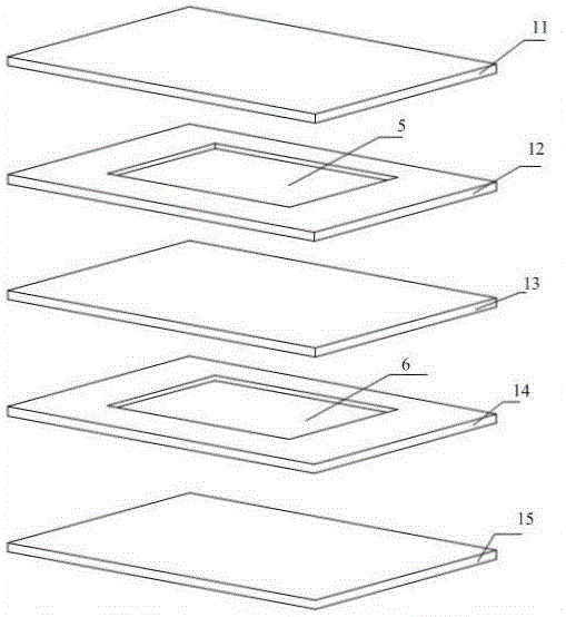
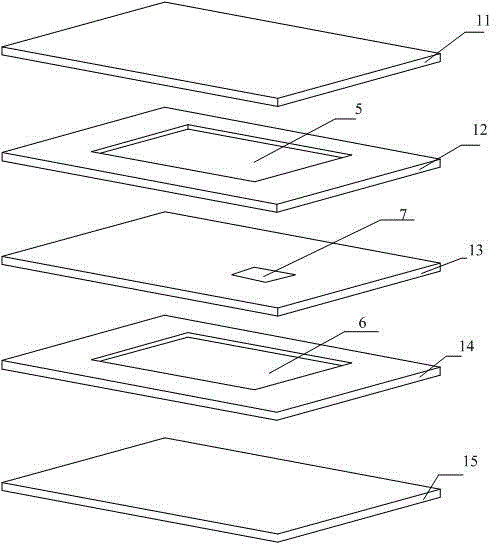
[0041] Embodiment 2: For the riveting realization of the suspension line circuit, when the number of circuit boards is 3, the 3 circuit boards are respectively the first circuit board 11, the second circuit board 12, the third circuit board 13, and the second circuit board Partially hollow out and cut out the local area of ​​the first circuit board 11 to form a hollow cavity A5, the metal layer on the reverse side of the first circuit board 11 covers the top of the hollow cavity A5, and the metal layer on the front side of the third circuit board 13 covers the bottom of the hollow cavity A5. The cavity A5 and the metal layer on the front side of the third circuit board 13 and the metal layer on the back side of the first circuit board 11 form an air cavity structure.

[0042] Further, in Implementation Mode 2, the device M can also be placed in the circuit structure, and the device M includes: electronic components or active devices or metamaterials or dielectric material struc...


PUM


Abstract

The invention discloses a multi-layer circuit board riveting structure, and a suspended line circuit constituted by the same, and a realization method for the suspended line circuit. The multi-layer circuit board riveting structure comprises at least two layers of circuit boards arranged in a laminated manner; each circuit board comprises a dielectric substrate and metal layers arranged on the front and back faces of the dielectric substrate; a multi-layer circuit board body is formed by the laminated circuit boards; rivet holes are formed in the multi-layer circuit board body; rivets are inserted in the rivet holes; the upper end parts of the rivets are press-fitted and riveted with the upper surface of the multi-layer circuit board body; and the lower end parts of the rivets are press-fitted and riveted with the lower surface of the multi-layer circuit board body.

Description

technical field [0001] The present invention relates to multilayer circuit board technology and suspension line circuit technology. A suspension line circuit formed by a circuit board riveting structure, and a method for realizing the suspension line circuit. Background technique [0002] With the development of radio frequency circuits and microwave and millimeter circuits, multilayer circuit structures have been extensively studied and applied in order to achieve superior circuit performance such as miniaturization and high integration of circuit structures. The multi-layer circuit structure can realize the miniaturization of the circuit structure, high integration and three-dimensional integration of active and passive circuits. In the multilayer circuit structure, the dielectric integrated suspension line and the common multilayer circuit board in the form of strip line and groove line need to be pressed by a certain device. The commonly used method of lamination of mu...

Claims


Application Information

Patent Timeline
Patent Type & Authority Applications(China)
IPC IPC(8): H05K1/02H05K3/46
CPCH05K1/0298H05K3/4611
Inventor 马凯学王勇强闫宁宁李连岳牟首先
Owner UNIV OF ELECTRONICS SCI & TECH OF CHINA
Why Eureka
Try Eureka