Pressure sensor of packaging structure and preparation method thereof

A technology of pressure sensor and packaging structure, which is applied in the direction of measuring fluid pressure by changing ohmic resistance, measuring fluid pressure, instruments, etc. It can solve the problems of complicated process and difficulty in mass production, and achieve simple packaging structure, which is conducive to long-term reliability Sex and stability, convenient and low-cost effect

Inactive Publication Date: 2015-12-23
CHINA ELECTRONIC TECH GRP CORP NO 38 RES INST
View PDF8 Cites 10 Cited by
  • Summary
  • Abstract
  • Description
  • Claims
  • Application Information

AI Technical Summary

Problems solved by technology

[0004] Chinese invention patent application: 201010295903.9, a gas pressure sensor; Chinese invention patent CN101271029A, a silicon piezoresistive pressure sensor packaging structure based on a substrate; both technologies use the method of pressure transmission to package the pressure sensor chip, Silicone gel is coated on the surface of the chip as a pressure transmission and protection isolation medium, but this packaging method, as pointed out by the above analysis, will have residual stress, which will generate excess stress due to inertial force, and the process is complicated and not easy to expand mass production

Method used


Image

  • Pressure sensor of packaging structure and preparation method thereof
  • Pressure sensor of packaging structure and preparation method thereof
  • Pressure sensor of packaging structure and preparation method thereof

Examples


Embodiment Construction

[0030] The embodiments of the present invention will be described in detail below. This embodiment is implemented on the premise of the technical solution of the present invention. Detailed implementation modes and specific operation procedures are given, but the protection scope of the present invention is not limited to the following implementations. example.

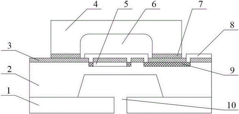
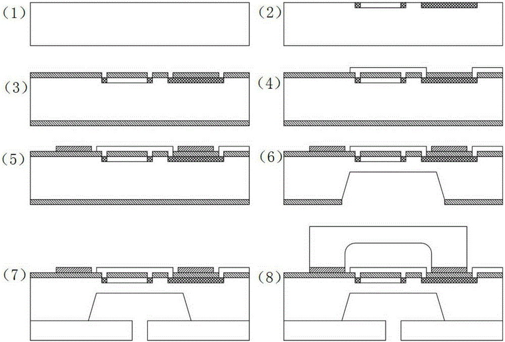
[0031] Such as image 3 As shown, this embodiment includes the following steps:

[0032] (1) Prepare substrate monocrystalline silicon wafer;

[0033] (2) Light boron doping and concentrated boron doping are performed on the front side of the monocrystalline silicon wafer to form a piezoresistive bar structure and a concentrated boron doped area;

[0034] (3) Deposit an insulating layer on both the front and back of the silicon wafer, and etch the piezoresistive bar and the electrical contact holes of the dense boron doped area on the front of the silicon wafer;

[0035] (4) Depositing a metal film on the insulating layer on t...


PUM

PropertyMeasurementUnit
thicknessaaaaaaaaaa
thicknessaaaaaaaaaa

Abstract

The invention discloses a pressure sensor of a packaging structure and a preparation method thereof. A lightly boron-doped region and a heavily boron-doped region are prepared by doping on the front of a silicon wafer. A groove is arranged on the back of the silicon wafer through etching. A silicon pressure film is formed between the bottom of the groove and the lightly boron-doped region. An insulating layer is laid on the front of the silicon wafer. A metal lead is arranged on the top of the insulating layer, and is connected with the lightly boron-doped region and the heavily boron-doped region. Four piezoresistive strips are formed in the lightly boron-doped region. The piezoresistive strips and the metal lead form a Wheatstone full-bridge structure. The front of the silicon wafer is bonded to a piece of front bonding glass through a middle layer. A piece of back bonding glass is bonded to the back of the silicon wafer, and the side, directly facing the silicon pressure film, of the back bonding glass is provided with an air guide hole. The part, directly facing the silicon pressure film, of the front bonding glass is provided with a cavity. The packaging structure of the invention is simple and compact, and highly reliable. The manufacturing process is simple, wafer level packaging can be realized, and low-cost mass production is facilitated.

Description

Technical field [0001] The invention relates to a MEMS piezoresistive pressure sensor, in particular to a pressure sensor with a package structure and a preparation method thereof. Background technique [0002] MEMS pressure sensor uses micro-film structure as the pressure sensitive unit, and is manufactured based on micro-nano processing technology. Compared with traditional pressure sensors, it has significant advantages such as small size, light weight, low power consumption, low cost, and suitable for mass production. , Has a wide range of applications in consumer electronics, automotive electronics, medical equipment, industrial control and other fields. MEMS pressure sensors can be divided into capacitive and piezoresistive types according to their principles. MEMS capacitive pressure sensors use the capacitance change caused by the deformation of the silicon pressure membrane as the output signal, while MEMS piezoresistive pressure sensors use the surface of the silicon pr...

Claims


Application Information

Patent Timeline
Patent Type & Authority Applications(China)
IPC IPC(8): G01L19/06G01L9/06
Inventor 曾鸿江胡国俊盛文军刘莹
Owner CHINA ELECTRONIC TECH GRP CORP NO 38 RES INST
Why Eureka
Try Eureka