Synchrotron radiation X-ray large-area interference lithography system

A technology of interference lithography and X-rays, which is applied in the field of synchrotron radiation X-ray large-area interference lithography system, can solve the problems of not meeting technical requirements, limiting the effective exposure area and large-area splicing, and achieving the effect of ensuring alignment accuracy

Active Publication Date: 2015-12-23
SHANGHAI INST OF APPLIED PHYSICS - CHINESE ACAD OF SCI
View PDF3 Cites 7 Cited by
  • Summary
  • Abstract
  • Description
  • Claims
  • Application Information

AI Technical Summary

Problems solved by technology

Taking nanomagnetism as an example, the measurement of the Kerr effect of a sample generally uses a variable-wavelength Kerr device, but the spot diameter of the current Kerr device is usually not less than 500 μm, and the experiment requires that the diameter of the measured area must be greater than or equal to 500 μm, so that the spot can be It is easy to focus on the pattern area, but the size of the pattern area obtained by XIL single exposure is far from meeting the technical requirements. Therefore, it is also necessary to splice multiple pattern areas to obtain a large and uniform pattern area to meet the requirements of the measuring instrument. Require
[0004] However, since the current XIL technology uses a diffraction grating as a mask to split the beam, such as figure 2 As shown, there will inevitably be a 0th-order (diffraction) light area 5' around the effective exposure area (i.e. ±1st-order diffracted light coherence area 4'), which limits the large-area splicing of the effective exposure area

Method used


Image

  • Synchrotron radiation X-ray large-area interference lithography system
  • Synchrotron radiation X-ray large-area interference lithography system
  • Synchrotron radiation X-ray large-area interference lithography system

Examples


Embodiment Construction

[0019] Below in conjunction with the drawings, preferred embodiments of the present invention are given and described in detail.

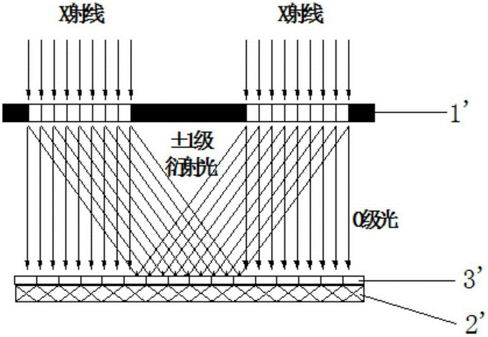
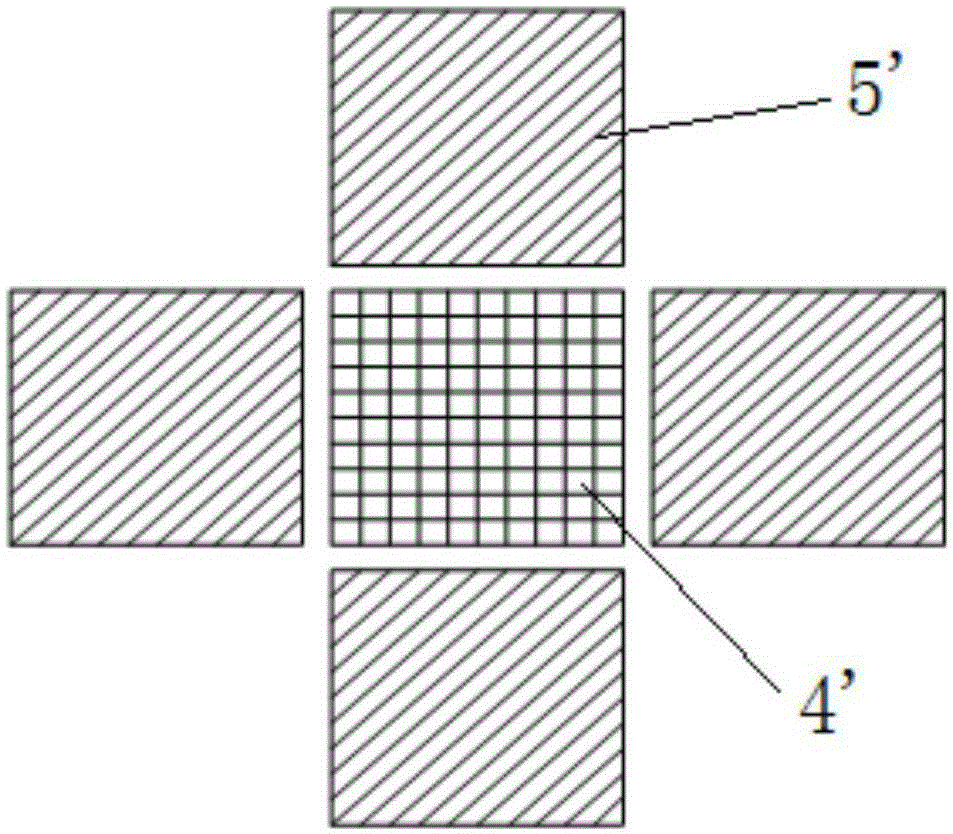
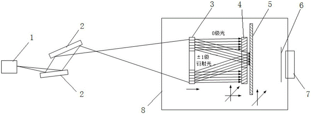
[0020] Such as image 3 As shown, the present invention, namely a kind of synchrotron radiation X-ray large-area interference lithography system, comprises: an undulator light source 1 arranged in sequence, a plurality of reflection focusing mirrors 2 (in this embodiment, the number of reflection focusing mirrors is 2), mask grating 3, gradation aperture 4 with aperture hole, sample stage 5 with observation hole, aluminum film 6 and CCD detector 7, also includes: first connected with gradation aperture 4 Mobile device (not shown in the figure) and the second mobile device (not shown in the figure) connected with sample stage 5; Wherein,

[0021] A plurality of reflective focusing mirrors 2 are configured to filter and transmit photons with energy above 1500eV in the X-ray emitted by the undulator light source 1 to the mask grating 3;

[0022] The...


PUM


Abstract

The invention relates to a synchrotron radiation X-ray large-area interference lithography system. The synchrotron radiation X-ray large-area interference lithography system comprises an undulator light source, multiple reflected focusing mirrors, a mask grating, a grading diaphragm with a diaphragm hole, a sample table with an observation hole, an aluminum film and a CCD (Charge Coupled Device) detector which are arranged in sequence. According to the synchrotron radiation X-ray large-area interference lithography system disclosed by the invention, position alignment between the mask grating and the grading diaphragm is ensured by additionally arranging the grading diaphragm between the mask grating and a sample and by means of the CCD detector, so that the grading diaphragm has the capability of reliably sheltering 0-grade light generated by beam splitting passing the mask grating to prevent the 0-grade light from irradiating the sample, and therefore no 0-grade light region exists around a + / -1 grade diffracted light coherent region generated on the sample; accordingly, large-area splicing of an effective exposure area on the sample can be realized by moving the sample table. Meanwhile, X-ray is filtered by adopting the reflected focusing mirrors and the aluminum film, so that a relative position of the mask grating and the grading diaphragm can be observed clearly by using the CCD detector, and therefore the alignment precision therebetween can be ensured.

Description

technical field [0001] The invention relates to a synchrotron radiation X-ray large-area interference photolithography system. Background technique [0002] X-ray interference lithography (XIL) is a new type of advanced micro-nano-processing technology that uses the interference fringes of two or more coherent X-beams to expose photoresists, and can carry out nanostructure processing of tens or even dozens of nanometer periods , its principle is as figure 1 As shown, the mask grating 1' divides a beam of X-rays into multiple beams of coherent beams, and produces interference fringes at the photoresist 3' on the substrate 2', thereby forming an exposure pattern. XIL technology is suitable for the preparation of large-area nano-periodic structures (ie, exposure patterns) with periods below 100nm. Compared with other methods such as photolithography, it can more reliably obtain large-area, high-quality sub-50nm high-density periodic nanostructures. , has a wide range of appli...

Claims


Application Information

Patent Timeline
Patent Type & Authority Applications(China)
IPC IPC(8): G03F7/20
Inventor 薛超凡吴衍青刘海岗杨树敏王连升赵俊邰仁忠
Owner SHANGHAI INST OF APPLIED PHYSICS - CHINESE ACAD OF SCI
Why Eureka
Try Eureka