Automatic verification platform and method for on-chip memory management unit fault-tolerant structure

A storage management unit and automatic verification technology, which is applied in the field of automatic verification platform of on-chip storage management unit fault-tolerant structure, can solve the problem of high chip testing cost, improve verification coverage, realize test data randomization, and realize test process automation Effect

Active Publication Date: 2015-12-23
NO 771 INST OF NO 9 RES INST CHINA AEROSPACE SCI & TECH
View PDF10 Cites 22 Cited by
  • Summary
  • Abstract
  • Description
  • Claims
  • Application Information

AI Technical Summary

Problems solved by technology

Although this method realizes the verification of SRAM FPGA fault tolerance combined with hardware and software, it needs its structure to implement fault injection and result comparison through dual FPGAs. Compared with FPGA2, if it is replaced with a chip, the test cost is higher

Method used


Image

  • Automatic verification platform and method for on-chip memory management unit fault-tolerant structure
  • Automatic verification platform and method for on-chip memory management unit fault-tolerant structure
  • Automatic verification platform and method for on-chip memory management unit fault-tolerant structure

Examples


Embodiment Construction

[0036] The present invention will be further described in detail below in conjunction with specific embodiments, which are explanations of the present invention rather than limitations.

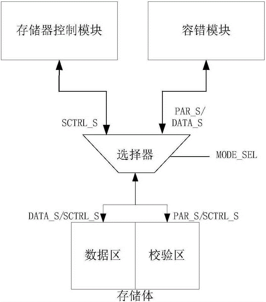
[0037] In the present invention, the fault-tolerant structure of the on-chip storage body adopts two modes of the memory working mode and the fault injection mode to control the data transmission path respectively, wherein in the working mode of the memory, the data area and the check area of ​​the storage body are taken as a whole, through a A set of control signals uniformly controls the input and output of data; in the fault injection mode, the data area and check area of ​​the memory bank are used as two independent storage areas to independently control data input and output through two sets of control signals, which is an on-chip memory bank. The random fault injection verification method of the fault-tolerant structure provides hardware support conditions.

[0038] Fault-tolerant struc...


PUM


Abstract

The invention provides an automatic verification platform and method for an on-chip memory management unit fault-tolerant structure. The automatic verification platform and method can conduct random fault injection verification on the fault-tolerant structure and are high in verification coverage rate. The platform comprises a debugging host and a to-be-tested host connected through a serial port. The debugging host is used for flow control verification, encoding result checking, fault injection, decoding result checking in the verification process, and monitoring and debugging of a processor. The on-chip memory stack fault-tolerant structure is integrated in the to-be-tested host and used for generation of check codes, decoding verification after decoding logic and fault injection and loading of an automatic verification program for the memory stack fault-tolerant structure. The memory stack fault-tolerant structure comprises a memorizer control module, a fault-tolerant module, a selector and a memory stack. The memorizer control module and the fault-tolerant module conduct read-write control over the memory stack through the selector to control the working mode and the failure mode of the on-chip memory stack fault-tolerant structure.

Description

technical field [0001] The invention relates to the field of fault testing of single event flipping, in particular to an automatic verification platform and method for fault-tolerant structures of on-chip storage management units. Background technique [0002] In recent years, with the rapid development of semiconductor technology, the demand for the scale and performance of integrated circuits has continued to increase. In order for SOC to be suitable for the deep space field, appropriate anti-radiation hardening technology must be adopted to solve the reliability problems caused by single event effects. [0003] The anti-flip and fault-tolerant design technology of the spaceborne system can only be verified on the ground to ensure the reliability of the design. The current methods are mainly through single-event irradiation test and simulation. The cost of single-event irradiation test is high. The cycle is long, and it is not easy to be used as an effective test method; t...

Claims


Application Information

Patent Timeline
Patent Type & Authority Applications(China)
IPC IPC(8): G11C29/08G06F17/50
Inventor 郭娜娜杨博刘虎兵楚亚楠谢琰瑾田超
Owner NO 771 INST OF NO 9 RES INST CHINA AEROSPACE SCI & TECH
Why Eureka
Try Eureka