Coarsened-sidewall AlGaInP-base LED and manufacture method thereof

A roughening, n-type technology, applied in electrical components, circuits, semiconductor devices, etc., can solve the problems of low light-emitting efficiency of AlGaInP-based LEDs, and achieve the effect of improving electro-optical conversion efficiency, reducing heat generation, and facilitating production and operation.

Active Publication Date: 2015-12-23
YANGZHOU CHANGELIGHT
View PDF10 Cites 25 Cited by
  • Summary
  • Abstract
  • Description
  • Claims
  • Application Information

AI Technical Summary

Problems solved by technology

[0006] Aiming at the above-mentioned problem that the light extraction efficiency of AlGaInP-based LEDs is very low due to the phenomenon of total reflection at

Method used


Image

  • Coarsened-sidewall AlGaInP-base LED and manufacture method thereof
  • Coarsened-sidewall AlGaInP-base LED and manufacture method thereof
  • Coarsened-sidewall AlGaInP-base LED and manufacture method thereof

Examples


Embodiment Construction

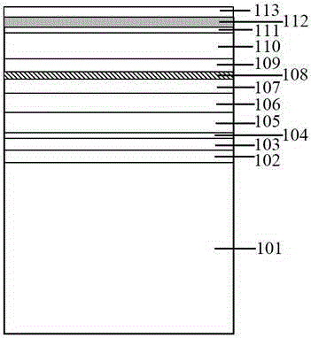
[0033] One, such as figure 1 and 2 Shown is the structural representation of the preferred example of the present invention in the manufacturing process, and the manufacturing steps are as follows:

[0034] 1. If figure 1 As shown, an epitaxial layer is grown on a GaAs temporary substrate 101 by MOCVD equipment, and the epitaxial layer includes a buffer layer 102, a GaInP cut-off layer 103, an n-GaAs ohmic contact layer 104, an n-AlGaInP roughening layer 105, and an n-AlGaInP current spreading layer. layer 106 , n-AlGaInP confinement layer 107 , MQW multiple quantum well active layer 108 , p-AlGaInP confinement layer 109 , p-GaP window layer 110 .

[0035] Wherein the n-GaAs ohmic contact layer 104 preferably has a thickness of 20nm to 100nm, and a doping concentration of 1×10 19 cm -3 Above, the doping element is Si, so as to form a good ohmic contact with the n-type extended electrode 204 . The preferred thickness of the p-GaP window layer 110 is 600nm to 8000nm, and th...


PUM


Abstract

The invention relates to a coarsened-sidewall AlGaInP-base LED and a manufacture method thereof and belongs to the technical field of semiconductors. The method comprises steps of: bonding an epitaxial wafer on a permanent substrate by using a metallic bonding layer on the epitaxial wafer and a metallic bonding layer on the permanent substrate in order to form a bonded semi-finished product; removing a temporary substrate, a buffer layer, and a cutoff layer on the bonded semi-finished product in order to expose an ohmic contact layer; etching and patterning the ohmic contact layer, and manufacturing a n-type expansion electrode, a main electrode, and a back electrode; and etching a cutting channel at least reaching a p-GaP window layer on the periphery of the epitaxial layer of each LED chip, coarsening the surface and the sidewall of the epitaxial layer in order that the surface and the sidewall of the epitaxial layer are coarsened. The manufacture method is simple in technology, convenient in production, and capable of increasing electro-optical conversion efficiency, prolonging the service life of the LED, enlarging a visual angle, and improving the display effect of an LED screen.

Description

technical field [0001] The invention relates to a structure and a manufacturing method of an AlGaInP-based LED with a roughened side wall, belonging to the technical field of semiconductors. Background technique [0002] The AlGaInP-based material that matches the GaAs substrate lattice is a direct bandgap semiconductor. By adjusting the ratio of Al and Ga, the forbidden band width can be changed between 1.9eV and 2.3eV, and the wavelength range of AlGaInP-based LEDs can cover 550nm -650nm. Therefore, AlGaInP-based materials have been widely used in the manufacture of red, orange, and yellow-green LEDs. Since the refractive index n of AlGaInP-based materials is as high as 3.0 to 3.5, it is much higher than conventional LED packaging materials such as epoxy resin and silica gel (n≈1.5). According to the law of total reflection of light, it can be seen that when light enters an optically thinner medium from an optically denser medium, total reflection will occur at the inter...

Claims


Application Information

Patent Timeline
IPC IPC(8): H01L33/22H01L33/00
CPCH01L33/0066H01L33/0093H01L33/22
Inventor 徐洲杨凯白继锋李俊承林鸿亮徐培强赵宇张永张双翔
Owner YANGZHOU CHANGELIGHT
Why Eureka
Try Eureka