

Method for depositing thick copper layers onto sintered materials
A technology of copper layer and sintered layer, applied in the field of electrodeposited copper layer to conductive sintered layer, can solve problems such as long processing time
- Summary
- Abstract
- Description
- Claims
- Application Information
AI Technical Summary
Problems solved by technology
Method used
Image

Examples
Embodiment 1
[0134] Example 1 : According to the present invention
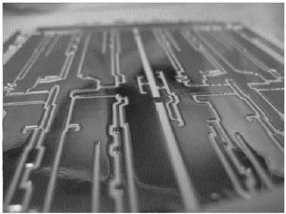
[0135] A ceramic substrate made of aluminum nitride having dimensions of 188 mm length and 137 mm width was used in the following examples. The substrate is covered with a conductive sintered layer comprising copper and titanium. The substrate is metallized according to the method of the invention.
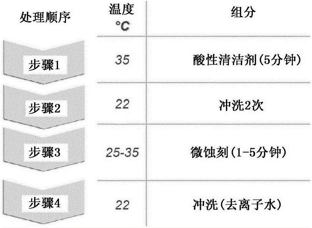
[0136] Table 3: Pretreatment order of substrates:
[0137]
[0138] The composition of the brine solution:
[0139]
[0140] After pretreatment, the substrate was subjected to electrodeposition of copper. First, use 1A / dm 2 Direct current of current density, pre-plating (corresponding to method step (ii.a)) of the substrate in the electrolytic copper deposition bath for 5 minutes. The substrate is then brought into contact with the electrolytic copper deposition bath and plated according to the following conditions (corresponding to method step (ii)). The electrolytic copper deposition bath is a conventional aci...
Embodiment 2
[0145] Example 2 : The present invention and comparative example
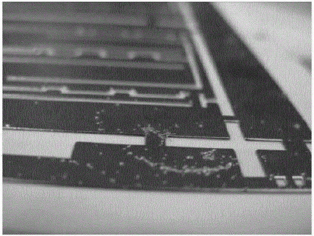
[0146] A ceramic substrate made of alumina having dimensions of 188 mm in length and 137 mm in width was used in the following examples. The substrate has a pattern of a conductive sintered layer made of silver-copper-titanium alloy. Thus, parts of the substrate are covered with the conductive sintered layer and other parts are free of sintered layer and present a bare ceramic surface. The parts that do not contain the sintered layer are therefore electrically insulated and are referred to as insulating regions or non-conducting regions. The substrates were pretreated by different pretreatment steps (i.aa); the overall sequence of the pretreatment steps is shown in Table 4. The pretreated substrate is metallized according to the method of the invention.
[0147] Table 4: Pretreatment sequence for this sintered layer
[0148]
[0149] Table 5: Preprocessing steps (i.aa)
[0150]
[0151] After pretr...
Embodiment 3
[0157] Embodiment 3: the present invention and comparative example
[0158] The internal stress of copper layers deposited according to the invention and from conventional copper deposition baths was measured. The copper electrodeposition bath of the present invention comprises copper (II) ions, sulfuric acid, chloride ions, a brightening agent, a leveling agent with a concentration range of 1-10 mg / l and a carrier with a concentration range of 0.2-2 g / l. This bath was used to plate substrates 4 to 6.
[0159] The conventional copper deposition baths used contain copper(II) ions, sulfuric acid, chloride ions and organic additives. This bath was used to plate substrates 7 to 9.
[0160] The substrate is a test strip for measuring stress. The substrate was pretreated with an acidic cleaner (CupraPro S8 Cleaner from Etotek Ltd.) for 1 minute and 10% w / v sulfuric acid for 30 seconds. The substrates were contacted with an electrolytic copper deposition bath and plated accordi...
PUM
| Property | Measurement | Unit |
|---|---|---|
| thickness | aaaaa | aaaaa |
| thickness | aaaaa | aaaaa |
| thickness | aaaaa | aaaaa |
Abstract
Description
Claims
Application Information