
Production method of film solar cell and electro-deposition device thereof

A technology for solar cells and production methods, applied in electrodes, circuits, electrical components, etc., can solve the problems of complex production process and high production cost of solar thin-film cells, and achieve the effects of saving processes, reducing waste and avoiding occupation.

Active Publication Date: 2015-12-30
BEIJING HI TECH WEALTH INVESTMENT DEV
View PDF7 Cites 4 Cited by
  • Summary
  • Abstract
  • Description
  • Claims
  • Application Information

AI Technical Summary

Problems solved by technology

[0015] For this reason, the technical problem to be solved by the present invention is that the production process of the solar thin film battery in the prior art is complicated, and the production cost is high, and then a kind of production process is simple, the production method of the low cost thin film solar battery and its electrodeposition device

Method used


Image

  • Production method of film solar cell and electro-deposition device thereof
  • Production method of film solar cell and electro-deposition device thereof
  • Production method of film solar cell and electro-deposition device thereof

Examples


Embodiment 1

[0089] This embodiment provides a method for producing a thin-film solar cell, comprising the following steps:

[0090] (a) if Figure 1b As shown, a transparent conductive layer 12 is formed on a glass substrate 11 .

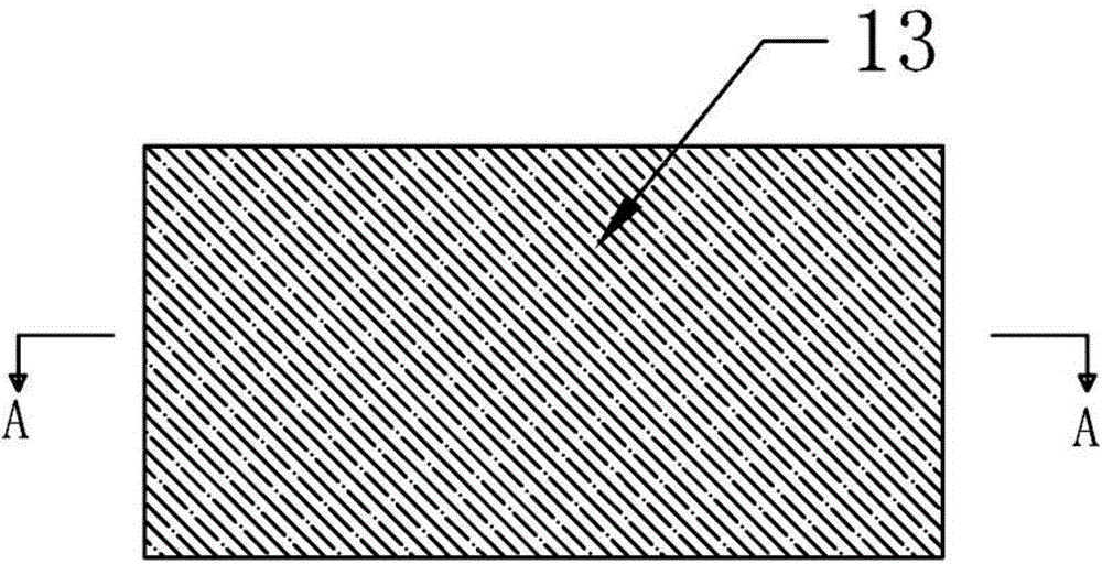
[0091] (b) if Figure 1a and 1b As shown, a window layer 13 is formed on the transparent conductive layer 12, and the window layer 13 is a cadmium sulfide (CdS) layer.

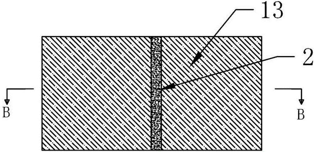
[0092] (c) if Figure 1c and 1dAs shown, the strip contact electrode 2 penetrates the window layer 13 and makes ohmic contact with the transparent conductive layer 12, the contact surface between the strip contact electrode 2 and the transparent conductive layer 12 is strip-shaped, and the strip contact surface The cross section of the strip contact electrode 2 perpendicular to the direction of the contact long side is rectangular, and the long side of the strip contact electrode 2 is a straight line.

[0093] (d) if Figure 1e As shown, on the transparent conductive layer 12 in step (c),...

Embodiment 2

[0106] This embodiment provides a method for producing a thin-film solar cell, the specific method is the same as that in Embodiment 1, the only difference is that the cross-section of the elongated contact electrode 2 perpendicular to the direction in which the elongated contact electrode 2 contacts the long side is circular, Specific as Figure 2d-2j shown.

[0107] Such as Figure 8a and Figure 8b As shown, in the electrodeposition tank, when the absorber layer 14 is electrodeposited on the window layer 13 and simultaneously fills the first groove P1, the elongated contact electrode 2 is connected and energized at the end.

[0108] As an alternative embodiment, in the production method of the thin film solar cell described in this embodiment, the cross-section of the elongated contact electrode perpendicular to the direction of the long side of the elongated contact electrode is trapezoidal

Embodiment 3

[0110] The production method of the thin-film solar cell described in this embodiment, the specific embodiment is the same as embodiment 1, the difference is:

[0111] In step (c), the elongated contact electrode 2 penetrates the window layer 13 and makes ohmic contact with the transparent conductive layer 12, and the contact surface between the elongated contact electrode 2 and the transparent conductive layer 12 is elongated, Such as Figure 3c As shown, the long side of the strip contact electrode 2 is a curve; as Figure 3d As shown, the cross section of the elongated contact electrode 2 perpendicular to the direction of the long side of the contact is trapezoidal, and the end of the elongated contact electrode 2 is connected with electricity.

[0112] In step (h), the back electrode layer is formed after filling the vacancy of the elongated contact electrode of the semi-finished product obtained in step (g). Formed by deposition, the second contact electrode is in ohmic...


PUM


Abstract

The invention provides a production method of a film solar cell. A first groove is filled with a substance identical with an absorption layer, and the substance of the absorption layer is a semiconductor; the vacancy of a long-strip-shaped contact electrode is directly filled with a substance identical with a back electrode, and the direct contact resistance between the back electrode and the absorption layer is very large, so that no influenced are caused to serial connection of solar cell units; and that is to say, the film solar cell does not need to be filled by an electrical-isolation substance, the electrical-isolation substance does not participate in photoelectric conversion, and the area of a dead area is reduced, so that the occupation of the solar cell by the electrical-isolation substance is avoided, and the photoelectric conversion area of the solar cell is increased. In addition, when the used contact electrode is the long-strip-shaped contact electrode, the long-strip-shaped contact electrode is removed after electro-deposition, then a long-strip-shaped contact electrode vacancy is obtained, and the original groove etching process is omitted, so that the wastes of production materials are reduced, the processes are saved, and the production cost is further lowered.

Description

technical field [0001] The invention relates to a thin-film solar cell, in particular to a production method of the thin-film solar cell and an electrodeposition device thereof. Background technique [0002] Solar cells, also known as "solar chips" or photovoltaic cells, are devices that directly convert light energy into electrical energy through the photoelectric effect or photochemical effect. Among them, thin-film solar cells based on the photoelectric effect are the main ones. [0003] Generally, thin-film solar cells are placed facing the sunlight upwards, and mainly include lower encapsulation layer, base layer, back electrode layer, back contact layer, absorber layer, window layer, upper contact layer and upper encapsulation layer from bottom to top. Chinese patent CN101807622A discloses a method for preparing a cadmium telluride thin-film solar cell module, which includes the following steps: [0004] First, deposit CdS film on transparent conductive film glass to...

Claims


Application Information

Patent Timeline
IPC IPC(8): H01L31/18C25D17/12
CPCY02P70/50
Inventor 张征宇李伟中
Owner BEIJING HI TECH WEALTH INVESTMENT DEV
Learn More