

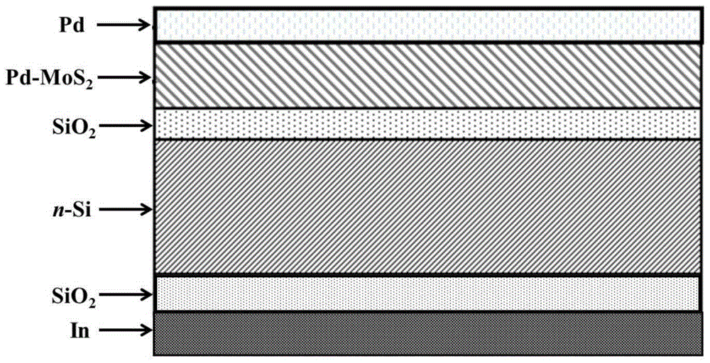
Pd-MoS2 heterojunction photovoltaic solar cell device and preparation method thereof
A solar cell, pd-mos2 technology, applied in photovoltaic power generation, electrical components, semiconductor devices, etc., can solve the problems of improving the axial conductivity of MoS2, not taking effective technical methods, low short-circuit current density, etc., and achieving good thermal stability. performance and chemical stability, improved photoconversion efficiency, and reduced defect density
- Summary
- Abstract
- Description
- Claims
- Application Information
AI Technical Summary
Problems solved by technology
Method used
Image

Examples
Embodiment 1
[0062] The preparation method is as follows:
[0063] The first step, Pd-MoS 2 Target preparation steps
[0064] Take 1 part of Pd metal particles with a purity of 99.99% or more and MoS with a purity of 99.9% or more according to the mole fractions 2 99 parts of particles, blended and pulverized into a ball mill to a particle size of 500-800 mesh powder;
[0065] Put the powder obtained by grinding into a tablet press mold and place it on the tablet press. The pressure of the press is 20-25MPa, the pressing time is 1 hour, and it is pressed into a cylindrical target with a thickness of 3-5mm and a diameter of 60mm. material;
[0066] The second step is the passivation step of the silicon substrate surface
[0067] Select an n-type Si single crystal substrate with a resistivity of 1-10Ω·cm and a crystal plane orientation of (100) planes, and ultrasonically clean them in alcohol, acetone and deionized water for 180s in sequence;
[0068] Take it out and place it in a hydrofluoric acid so...
Embodiment 2
[0081] (Note: This example is a comparative example, the target material used is pure MoS 2 Target. That is, in the preparation process of the target, Pb metal is not used to MoS 2 Doping treatment)
[0082] The first step, pure MoS 2 Target preparation steps
[0083] Take MoS with purity above 99.9% 2 The particles are pulverized into a ball mill to a particle size of 500-800 mesh powder;
[0084] Put the powder obtained by grinding into a tablet press mold and place it on the tablet press. The pressure of the press is 20-25MPa, the pressing time is 1 hour, and it is pressed into a cylindrical target with a thickness of 3-5mm and a diameter of 60mm. material;
[0085] The rest are the same as in Example 1.
[0086] Product performance test results:
[0087] After testing, at 30mWcm -2 Under the white light conditions, the prepared MoS 2 The light excitation current density of the heterojunction photovoltaic solar cell device is 3.5mAcm -2 , The open circuit voltage is 0.23V, and the c...
Embodiment 3
[0089] The first step, Pd-MoS 2 Target preparation steps
[0090] Take 0.5 parts of Pd metal particles with a purity of 99.99% or more and MoS with a purity of 99.9% or more according to the mole fractions 2 99.5 parts of particles, blended and pulverized into a ball mill to a particle size of 500-800 mesh powder;
[0091] Put the powder obtained by grinding into a tablet press mold and place it on the tablet press. The pressure of the press is 20-25MPa, the pressing time is 1 hour, and it is pressed into a cylindrical target with a thickness of 3-5mm and a diameter of 60mm. material;
[0092] The rest are the same as in Example 1.
[0093] Product performance test results:
[0094] After testing, at 30mWcm -2 Under the white light conditions, the Pd-MoS prepared 2 The light excitation current density of the heterojunction photovoltaic solar cell device is 5.2mAcm -2 , The open circuit voltage is 0.33V, and the conversion efficiency is 2.8%.
PUM
| Property | Measurement | Unit |
|---|---|---|
| Thickness | aaaaa | aaaaa |
| Particle size | aaaaa | aaaaa |
| Resistivity | aaaaa | aaaaa |
Abstract
Description
Claims
Application Information