Check patentability & draft patents in minutes with Patsnap Eureka AI!

OLED display pixel circuit and driving method thereof

A technology for displaying pixels and pixel driving circuits, which is applied in the field of flat-panel displays, can solve the problems of AMOLED pixel circuit structure complexity and difficulty in driving, and achieve the effects of simple driving sequence, avoiding IC design, and simplifying circuit structure

Active Publication Date: 2016-01-27
PEKING UNIV
View PDF4 Cites 28 Cited by
  • Summary
  • Abstract
  • Description
  • Claims
  • Application Information

AI Technical Summary

Problems solved by technology

[0004] The present invention aims to solve the problem that the structure of AMOLED pixel circuit is complicated and it is difficult to drive it, and proposes a pixel circuit based on a double-gate structure TFT

Method used


Image

  • OLED display pixel circuit and driving method thereof
  • OLED display pixel circuit and driving method thereof
  • OLED display pixel circuit and driving method thereof

Examples


Embodiment 1

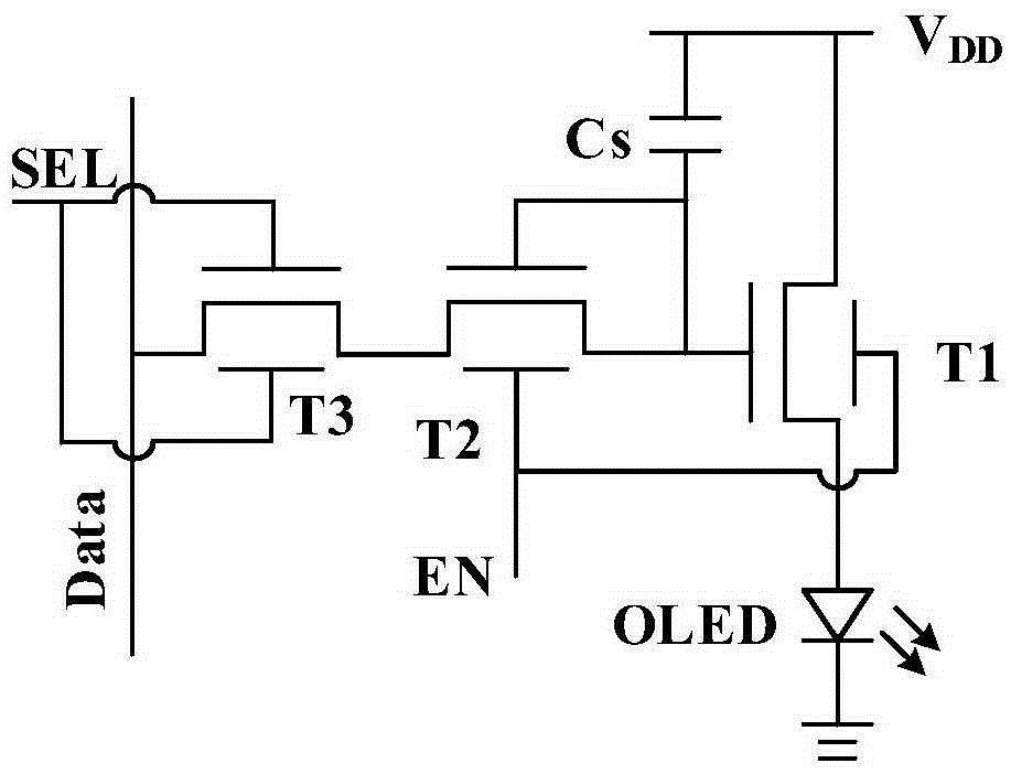
[0035] The pixel driving circuit of the present invention includes: figure 1 As shown, the first transistor T1, the second transistor T2, the third transistor T3, the storage capacitor Cs and the organic light emitting diode OLED;

[0036] Wherein, the first transistor T1 is a double-gate thin film transistor, its first gate electrode is connected to the drain of the second transistor T2, the first gate electrode of the second transistor T2 and one end of the storage capacitor; its second gate electrode is connected to the second transistor T2 The second gate electrode of T2 is connected to a gate control line EN; its drain and one end of the storage capacitor Cs are connected to the power line V DD ; Its source is connected to the anode of the organic light emitting diode OLED.

[0037] The second transistor T2 is a double-gate thin film transistor, its first gate electrode and drain are connected together with one end of the storage capacitor and the first gate electrode of...

Embodiment 2

[0053] The pixel driving circuit of the present invention includes: Figure 5 As shown, the first transistor T1, the second transistor T2, the third transistor T3, the storage capacitor Cs and the organic light emitting diode OLED;

[0054] Wherein, the first transistor T1 is a double-gate thin film transistor, and the first gate electrode is connected to the drain of the second transistor T2, the first gate electrode of the second transistor T2 and one end of the storage capacitor; the second gate electrode of the first transistor T1 and The second gate electrode of the second transistor T2 is connected to a gate control line EN; the drain of the first transistor T1 is connected to the cathode of the organic light emitting diode OLED; the anode of the organic light emitting diode OLED is connected to one end of the storage capacitor and connected to the power line V DD ; The source of the first transistor T1 is connected to the ground port.

[0055] The second transistor T2 ...

Embodiment 3

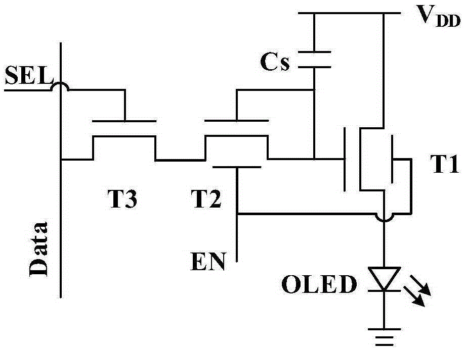
[0062] The pixel driving circuit of the present invention includes: Figure 1-3 Or as shown in 5-7, the first transistor T1, the second transistor T2, the third transistor T3, the storage capacitor Cs and the organic light emitting diode OLED;

[0063] Wherein, the first transistor T1 is a double-gate TFT; the second transistor T2 is a TFT with a double-gate structure; the third transistor T3 can be a double-gate TFT or a single-gate TFT. The anode of the organic light emitting diode OLED is connected to the source of the first transistor T1, and the cathode is connected to the ground port. The connection mode of the second transistor and the third transistor and the organic light-emitting diode OLED is the same as that in Embodiment 1 (as shown in the appended Figure 1-3 shown); the drain of the first transistor T1 is directly connected to the power line; one end of the storage capacitor Cs is connected to the first gate electrode of the first transistor T1, the first gate ...


PUM


Abstract

The invention discloses a pixel drive circuit and a driving method thereof. The pixel drive circuit is composed of a first transistor, a second transistor, a third transistor, a storage capacitor, an organic light-emitting diode (OLED), a power line, a data signal line, and a gate control line. The transistors employ dual-gate-structure-based TFTs; and on the basis of the characteristic of threshold voltage adjustability of the dual-gate TFT, compensation of the threshold voltage drift phenomenon can be realized and the stable output current can be provided, so that a problem of non-uniform brightness of the OLED luminescent device due to uneven threshold voltage or threshold voltage drift of the TFT display panel can be effectively solved. Meanwhile, because the dual-gate-structure-based TFTs have high current and device stability, the low-working-voltage operation of the circuit can be realized and the smaller area is realized. The circuit structure is simplified; the aperture opening ratio and resolution rate of the display circuit are improved; and the manufacturing cost is lowered. The pixel drive circuit with a high practical value can be widely applied to the micro-electronics and panel display industry.

Description

technical field [0001] The invention belongs to the technical field of flat panel display, and in particular relates to an OLED display pixel drive circuit and a drive method for the pixel circuit thereof. Background technique [0002] Active Matrix Organic Light-Emitting Diode (AMOLED) display is considered to be the next-generation mainstream display technology due to its advantages of fast response, high brightness, high contrast, low power consumption, and easy realization of flexibility and transparency. The active matrix is ​​a pixel circuit array composed of thin film transistors (ThinFilmTransistor, TFT), which is a key part of AMOLED display. At present, the TFT technologies used for AMOLED driving mainly include amorphous silicon TFT, low-temperature polysilicon TFT and emerging metal oxide TFT. However, these three TFT technologies all have defects such as threshold voltage drift and uneven threshold voltage; making them unable to provide stable and uniform curre...

Claims


Application Information

Patent Timeline
Patent Type & Authority Applications(China)
IPC IPC(8): G09G3/3258
Inventor 王漪伦志远丛瑛瑛赵飞龙董俊辰韩德栋
Owner PEKING UNIV
Features
  • R&D
  • Intellectual Property
  • Life Sciences
  • Materials
  • Tech Scout
  • Unparalleled Data Quality
  • Higher Quality Content
  • 60% Fewer Hallucinations
Learn More