A kind of magnetic tunnel junction and its preparation method
A technology of magnetic tunnel junction and magnetic layer, applied in the field of magnetic tunnel junction and its preparation, can solve the problems of inability to take into account the small device size and thermal stability compatibility at the same time, and achieve shortened annealing time, high small size and high vertical The effect of magnetic anisotropy
- Summary
- Abstract
- Description
- Claims
- Application Information
AI Technical Summary
Problems solved by technology
Method used
Image
Examples
preparation example Construction
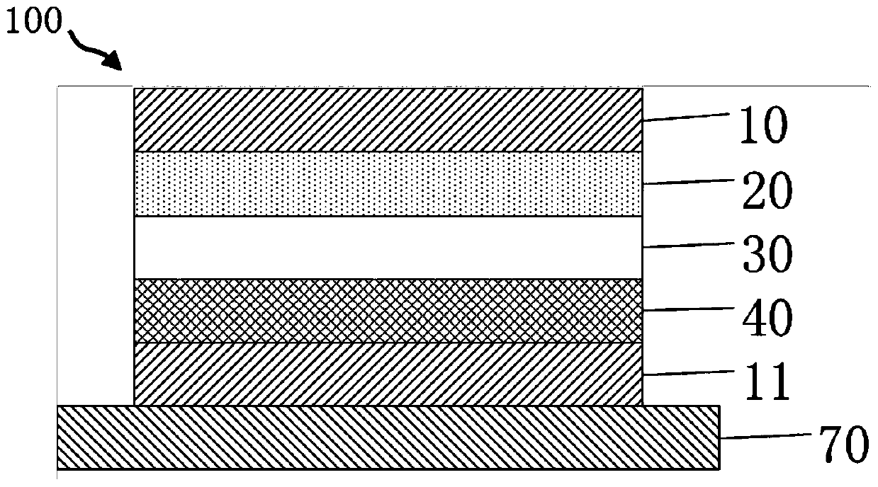
[0033] The preparation method of the above-mentioned magnetic tunnel junction comprises the following steps:
[0034] (1) depositing the first electrode material on the substrate 70, and patterning to obtain the first electrode layer 11;
[0035] (2) sequentially depositing a first magnetic material, an insulating material and a second magnetic material on the first electrode layer 11, and patterning to obtain a first magnetic layer 40, an insulating tunneling layer 30 and a second magnetic layer 20;
[0036] (3) depositing a second electrode material on the second magnetic layer 20, and patterning to obtain the second electrode layer 10;
[0037] (4) Annealing at 300-500° C. for 5-10 minutes to obtain a magnetic tunnel junction.
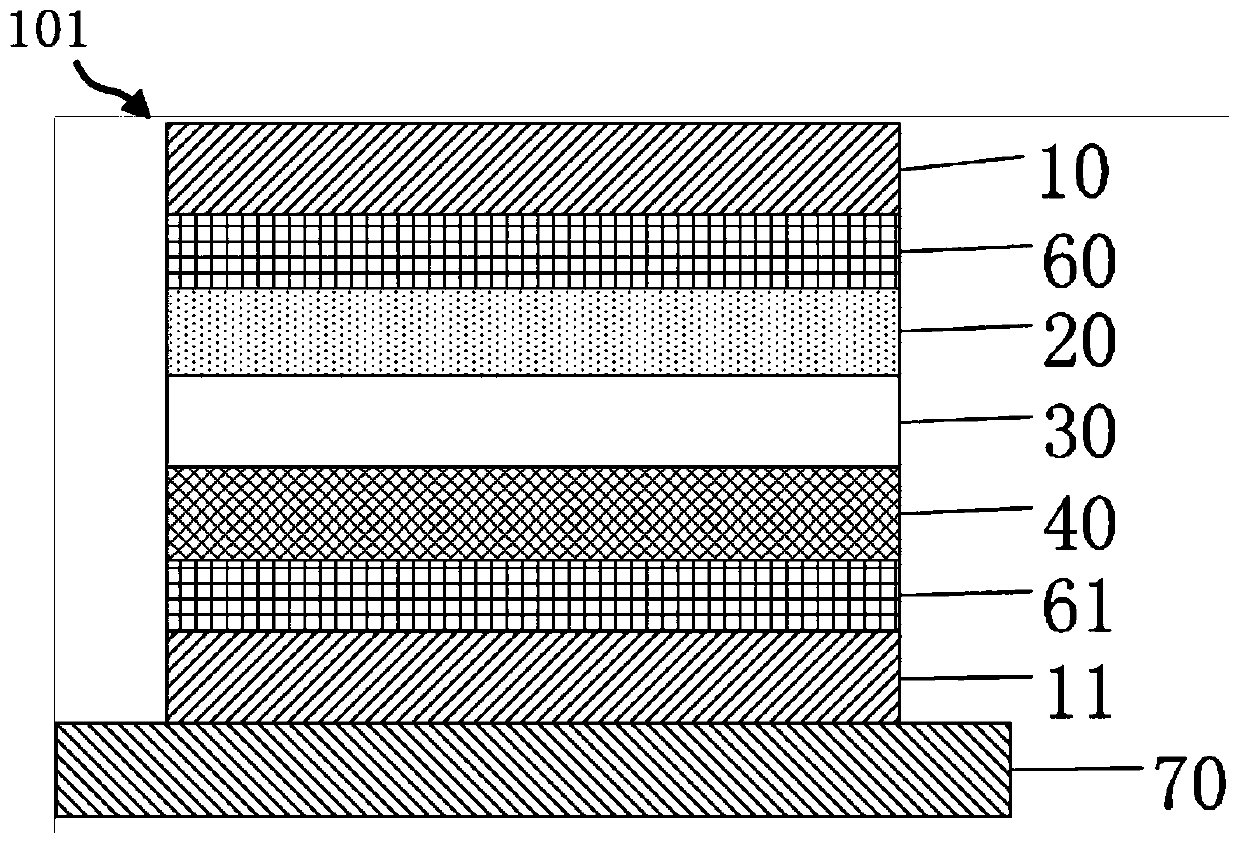
[0038] Wherein, the first electrode material is obtained by sequentially depositing FePt and CoFe(R), and / or the second electrode material is obtained by sequentially depositing CoFe(R) and FePt, CoFe(R) is CoFe doped with R, R is B, At least one ...
Embodiment 1
[0041] combine figure 1 , the preparation method of the above-mentioned magnetic tunnel junction comprises the following steps:
[0042] Step 101: providing a substrate 70, the substrate 70 is a thermally oxidized Si sheet or a CMOS chip;
[0043] Step 102: In an argon atmosphere, the first electrode layer 11 is prepared on the substrate 70 by magnetron sputtering, the deposition temperature is room temperature, the target material is Cu, and the vacuum degree is better than 10 -6 Pa, the thickness of the first electrode layer 11 is 200nm;
[0044] Step 103: In an argon atmosphere, the first magnetic layer 40 is prepared on the first electrode layer 11 by magnetron sputtering, which includes depositing a FePt layer on the first electrode layer 11 with a thickness of 3 nm, and then depositing CoFeB layer, the thickness is 5nm, the deposition temperature is room temperature, and the targets are Fe 50 Pt 50 alloy target and Co 40 Fe 40 B 20 target, the vacuum degree is bet...
Embodiment 2
[0052] The thickness of the FePt layer is 4.5nm, the thickness of the CoFeB layer is 5nm, and other steps are the same as in Embodiment 1.
PUM
 Abstract
Description
Claims
Application Information


